
Industry Directory | Training Provider / Manufacturer's Representative / Equipment Dealer / Broker / Auctions / Consultant / Service Provider
Products, services, training & consulting for the assembly, rework & repair of electronic assemblies. BGA process experts. Manufacturers Rep, Distributor & Service Provider for Seamark/Zhuomao and Shuttle Star BGA Rework Stations.
Industry Directory | Manufacturer
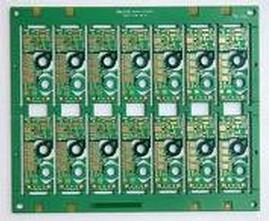
Caring Circuit specialises in the supply of prototype, small and medium-series PCBs factory in Shenzhen,China.We are a leading provider of custom Single layer,double layer,multilayer rigid PCBs.
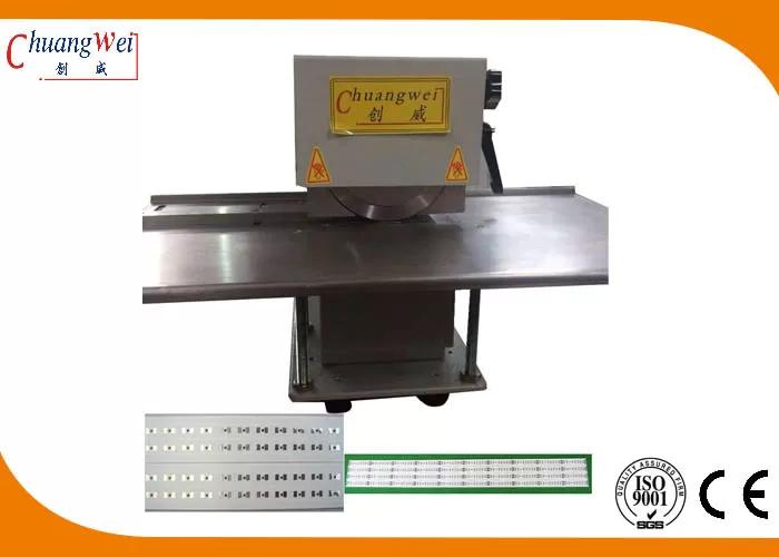
Specification for pcb cutting machine Model CWVC-1S Max cutting length unlimited platform length 1.2 / 2.4 m can be according to sustomer's requirement PC
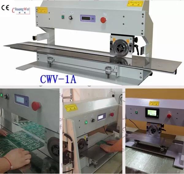
PCB Separator machine advantages : 1. Easy maintanance and operation 2. Low bending stress,no vibration 3. specially for resin substrate PCB with pre-scored V groove 4. safety use PCB Separators Specifications : Model CWV-1A
Electronics Forum | Wed Sep 12 03:52:45 EDT 2018 | shascoet29
Hi, Is the IPC-A-610 applicable to CSP assemblies? Especially regarding the solder ball to solder ball distance versus the minimum electrical clearance for assembly(0.13mm/IPC-A-610). With a 0.4mm pitch component and 260 microns diameters balls, thi
Electronics Forum | Tue Jun 06 11:57:12 EDT 2006 | Chunks
IPC 610 says acceptable Class 1 (Class 2, 3 indicator) if they are entrapped/encpsulated balls within 0.13mm of lands or pads. or exceed 0.13mm in diameter. Defect Class 1,2,3: Solder ball violates min electrical clearance. Solder balls not entrap
Used SMT Equipment | Screen Printers
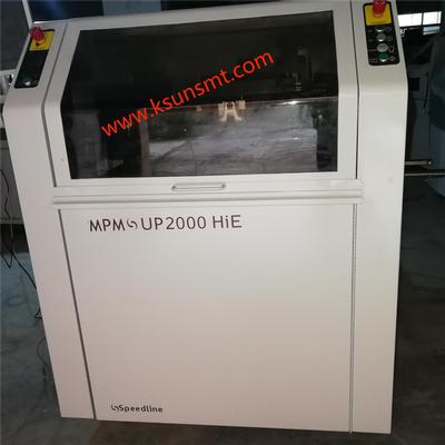
MPM UP2000HiE PRINTER Substrate treatment Minimum/maximum size 2"x 2"(50.0 mm x50.0 mm) to 20" x 16" (508 mm x 406 mm)(16 "or larger substrate requires special clamps) Thickness rang

Used SMT Equipment | Flexible Mounters
Product Name: Samsung SM481 high speed chip mounter Product number: SM481 Detailed product introduction Samsung SM481 high speed chip mounter parameters SM481 is based on the platform of high-speed SMT SM471 the fastest equipment at strengthening
Industry News | 2003-05-22 08:36:27.0
Packaging Saves PCB Board Space Without Sacrificing Power Dissipation Capability
Industry News | 2018-04-15 20:01:15.0
SMTA Europe announces Session 4 Technical Program on Electrochemical Reliability at the “Electronics in Harsh Environments Conference” to be held in Amsterdam, Netherlands, on April 25th, 2018.
Parts & Supplies | Assembly Accessories
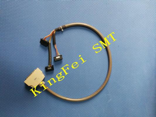
Detailed Product Description Part Name: LNC60 I/F Cable ASM Part Number: 40070445 Machine: JUKI KE2070 2080 FX3 Machine Condition: Original New Brand: JUKI Application: For LNC60 Laser 40070445 LNC60 I/F Cable ASM(2012) For JUKI 2070 2080 FX3 Mac
Parts & Supplies | Circuit Board Assembly Products
PULANG TECHNOLOGY CO,.LTDOffers electronic manufacturing services including PCB designing, electronic contract manufacturing including electronic product design, electronic product development, electronic product repair, PCB manufacturing, electronic
Technical Library | 2023-05-02 19:03:34.0
The demand for 0201 components in consumer products will increase sharply over the next few years due to the need for miniaturization. It is predicted that over 20 billion 0201 components will be used in more than one billion cell phones worldwide by the year 2003. Therefore, research and development on 0201 assembly is becoming a very hot topic. The first step to achieve a successful assembly process is to obtain a good PCB design for 0201 packages. This paper presents the data and criteria of PCB design for 0201 packages, including the pad design for 0201 components, and the minimum pad spacing or component clearance between 0201 components or between 0201 and other components. A systematic study on pad design and pad spacing was undertaken, using two test vehicles and three Design of Experiments (DOEs). In the first DOE, 2 out of 18 types of 0201 pad designs were selected based on process yield. The second DOE was focused on pad spacing, including 10mil, 8mil, 6mil and 4mil. The third experiment was final optimization, using two types of optimized pad designs with 10mil, 8mil and 6mil pad spacing. Through the above experiments, the design guideline for PCB layout for 0201 packages and the assembly process capability are identified.
Technical Library | 2022-12-19 18:59:51.0
Material and Process Characterization studies can be used to quantify the harmful effects that might arise from solder flux and other process residues left on external surfaces after soldering. Residues present on an electronic assembly can cause unwanted electrochemical reactions leading to intermittent performance and total failure. Components with terminations that extend underneath the package can trap flux residue. These bottom terminated components are flush with the bottom of the device and can have small solderable terminations located along the perimeter sides of the package. The clearance between power and ground render high electrical forces, which can propagate electrochemical interactions when exposed to atmospheric moisture (harsh environments). The purpose of this research is to predict and understand the functional performance of residues present under single row QFN component packages. The objective of the research study is to develop and collect a set of guidelines for understanding the relationship between ionic contamination and electrical performance of a BTC component when exposed to atmospheric moisture and the trade-offs between electrical, ionic contamination levels, and cleanliness. Utilizing the knowledge gained from undertaking the testing of QFN components and associated DOE, the team will establish a reference Test Suite and Test Spec for cleanliness.
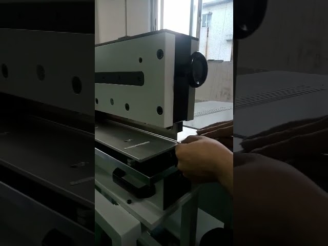
Guillotine type V-cut PCB Cutting Machine Product Description 1. For internal strength generates during separation, Minimize it to value under 180uE ,to avoid solder crack or component damage 2. Able to separate edge of V-slot, minimum distance to
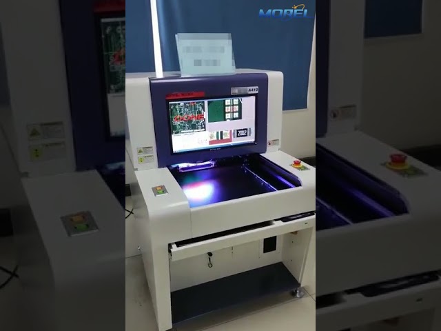
ML-A410 SMT Automated Optical Inspection Machine Feature ▶Economical and practical AOI. ▶High precision detection platform design. ▶Fast programming debugging integration. ▶Automatic recognize the Tip and Bottom side. ▶Professional SPC system.
Training Courses | | | Other Courses
Other courses related to electronics manufacturing and assembly
Training Courses | | | PCB Design Courses
The PCB design courses teach students the process, techniques and tools needed to design layout of printed circuit boards.
Career Center | Lancaster, Pennsylvania USA | Engineering
Provide leadership to the engineering staff and manage, initiation and completion of all engineering deliverables. Deal with customers, business associates, program managers, manufacturing, planning, marketing and purchasing. Requires extensive kno
Career Center | Fremont, California USA | Engineering
Interprets electrical design requirements and uses Allegro design tool to create original PCB layouts, detailed fab drawings, schematics, and other design files. Work with HW design engineer to make sure PCB layout meet PCB design requirements.
Career Center | Pune, Maharahtra India | Engineering,Maintenance,Technical Support
SMT Test Engineer/Electrical Automation Engineer. Good exposure on Agilent, Vitrox, Vi tech and TRI Aoi,s Good exposure on agilent ICTS and DAGE X rays.
Career Center | Erode, Tamilnadu India | Engineering
Professional Summary 3+ years of experience in the PCB CAM engineering Exposure to FRONTLINE GENESIS 2000 Having exposure in UCAM Exposure to Create, Array & Panelize it for manufacturability Experienced in Creating impedance cou
KingFei SMT Tech | http://www.smtspare-parts.com/sale-9135913-japan-origin-ipulse-m018-smt-nozzle-m1-m4-nozzle-for-electrical-machine.html
Japan Origin Ipulse M018 SMT Nozzle M1/ M4 Nozzle For Electrical Machine Leave a Message We will call you back soon! Your message must be between 20-3,000 characters
| https://www.feedersupplier.com/sale-13118784-smt-machine-original-new-electrical-ss-feeder-8mm-for-yamaha-pick-and-place-machine-khj-mc100-000-kh.html
SMT machine Original New electrical SS feeder 8mm for YAMAHA pick and place machine KHJ-MC100-000 KHJ-MC100-006 Leave a Message We will call you back soon
Products, services, training & consulting for the assembly, rework & repair of electronic assemblies. BGA process experts. Manufacturers Rep, Distributor & Service Provider for Seamark/Zhuomao and Shuttle Star BGA Rework Stations.
Training Provider / Manufacturer's Representative / Equipment Dealer / Broker / Auctions / Consultant / Service Provider
1750 Mitchell Ave.
Oroville, CA USA
Phone: (888) 406-2830


