Industry Directory | Manufacturer
We provide cost effective, custom printed circuit boards (PCBs) through an instant online system. We also provide PCB Assemb
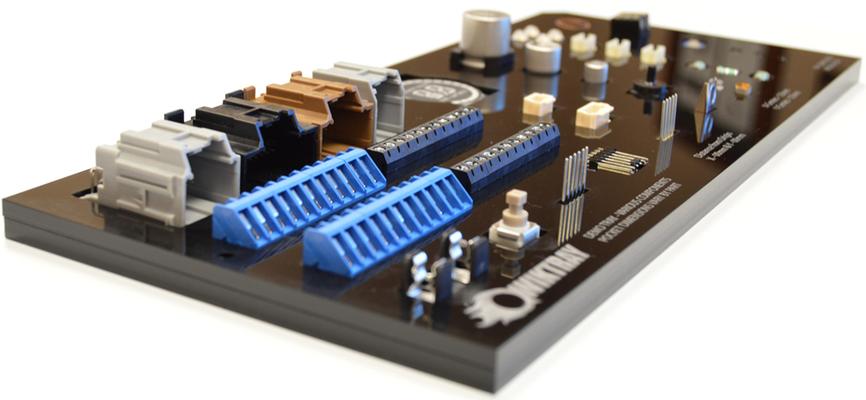
Do you have a unique component that isn’t available in tape and reel? Tired of hand placing those components because you don’t have a compatible feeder? Can’t find JEDEC trays for your components and you need one yesterday? The answer to all of
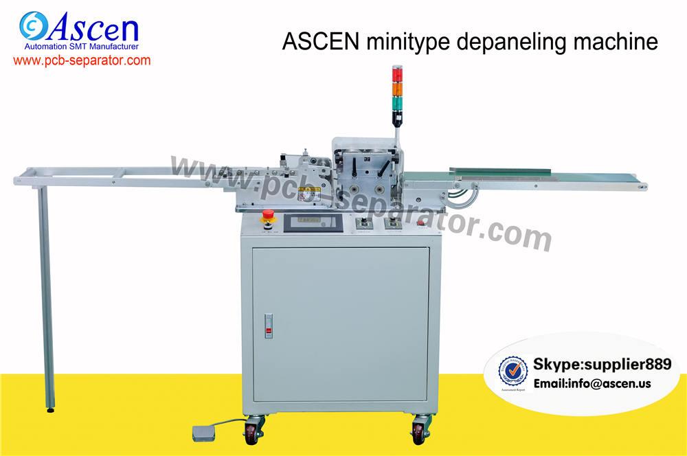
ASCEN-PCB multi cutter separator applies to automatic online separate the PCB board. At the same time, the minimum cutting length can achieve 100mm and no limits of the cutting length. High efficiency multi cutter PCB depeneling machine's minimu
Electronics Forum | Tue Feb 16 14:04:10 EST 2016 | tsvetan
We are designing board which have to plug in M.2 connector and thickness is limited to 0.8 mm The board is very complex with many BGAs and DDR3 memory chips and we will need 6 layers for routing. The problem is that we will need signals with 50, 90
Electronics Forum | Sat Oct 22 22:10:09 EDT 2011 | unisoft
Hi maybe this will help Rich larue rlarue@unisoft-cim.com ProntoGERBER-CONNECTION ( http://www.unisoft-cim.com/gerber_connection.htm ) imports raw Gerber data and allows the user to add intelligent information to the shapes on the display and c

Used SMT Equipment | Pick and Place/Feeders
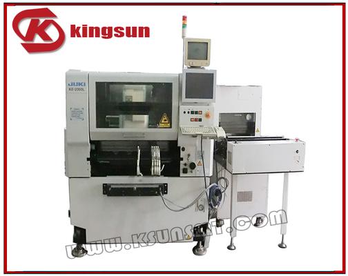
Product name: KE - 2060L JUKI chip mounter Product number: KE - 2060L JUKI2060 chip mounter parameters: Mounting head: 3 Material stand: 80 Mount speed: 0.25 SEC/CHIP (3 head at thesame time put in the attached SMT) Mounting speed:+ / - 0.. 5 M
Used SMT Equipment | SMT Equipment
Product name: KE - 2060 l JUKI chip mounter Product number: KE - 2060 l JUKI2060 chip mounter parameters: Mounting head: 3 Material stand: 80 Mount speed: 0.25 SEC/CHIP (3 head at the same time put in the attached SMT) Mounting speed:+ / - 0.
Industry News | 2017-10-02 13:58:42.0
GPD Global will exhibit at the upcoming IMAPS 2017. At booth 244, GPD Global will exhibit a complete line of Fluid Dispensing pumps with the latest dispense technologies for integration or retrofit. Whether your process requires low or high viscosity fluids, thick pastes, or abrasive media, there is a dispense pump to meet your requirements.
Industry News | 2018-10-18 11:08:03.0
Different Techniques for Plating
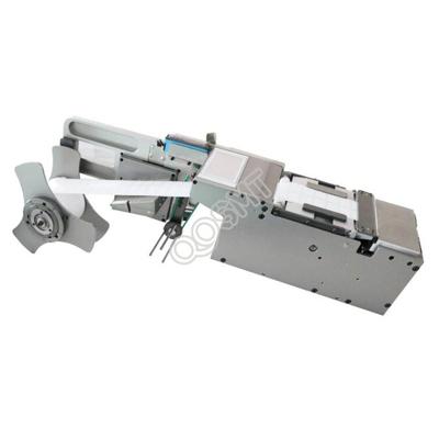
Parts & Supplies | Pick and Place/Feeders
Parameter Minimum Maximum Label Size 2 x 2mm ( Length x Width) 2mm to customized one (Width) Label Thickness 0.05mm 1mm Backing Paper Width 5mm (Width) 5mm to customized one (Width) Backing Paper Thickness 0.05mm 1mm Feed
Parts & Supplies | Pick and Place/Feeders
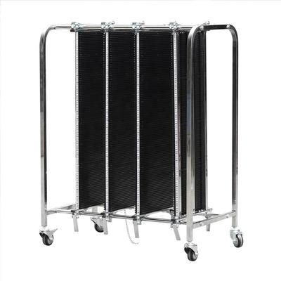
Place of Origin:Guangdong, China Usage:Storage Structure:Platform Material:Stainless Steel Wheel:Four-wheel Product name:pcb trolley Height can be placed/layer:280mm±10mm PP board thickness:10mm Available layer:3 Loading weight/layer:
Technical Library | 2023-07-25 16:25:56.0
This paper address two significant applications of stencils in advance packaging field: 1. Ultra-Thin stencils for miniature component (0201m) assembly; 2. Deep Cavity stencils for embedded (open cavity) packaging. As the world of electronics continues to evolve with focus on smaller, lighter, faster, and feature-enhanced high- performing electronic products, so are the requirement for complex stencils to assemble such components. These stencil thicknesses start from less than 25um with apertures as small as 60um (or less). Step stencils are used when varying stencil thicknesses are required to print into cavities or on elevated surfaces or to provide relief for certain features on a board. In the early days of SMT assembly, step stencils were used to reduce the stencil thickness for 25 mil pitch leaded device apertures. Thick metal stencils that have both relief-etch pockets and reservoir step pockets are very useful for paste reservoir printing. Electroform Step-Up Stencils for ceramic BGA's and RF Shields are a good solution to achieve additional solder paste height on the pads of these components as well as providing exceptional paste transfer for smaller components like uBGAs and 0201s. As the components are getting smaller, for example 0201m, or as the available real estate for component placement on a board is getting smaller – finer is the aperture size and the pitch on the stencils. Aggressive distances from step wall to aperture are also required. Ultra-thin stencils with thicknesses in the order of 15um-40um with steps of 15um are used to obtain desired print volumes. Stencils with thickness to this order can be potential tools even to print for RDLs in the package.
Technical Library | 2023-07-25 16:42:54.0
Printing solder paste for very small components like .3mm pitch CSP's and 01005 Chip Components is a challenge for the printing process when other larger components like RF shields, SMT Connectors, and large chip or resistor components are also present on the PCB. The smaller components require a stencil thickness typically of 3 mils (75u) to keep the Area Ratio greater than .55 for good paste transfer efficiency. The larger components require either more solder paste height or volume, thus a stencil thickness in the range of 4 to 5 mils (100 to 125u). This paper will explore two stencil solutions to solve this dilemma. The first is a "Two Print Stencil" option where the small component apertures are printed with a thin stencil and the larger components with a thicker stencil with relief pockets for the first print. Successful prints with Keep-Outs as small as 15 mils (400u) will be demonstrated. The second solution is a stencil technology that will provide good paste transfer efficiency for Area Ratio's below .5. In this case a thicker stencil can be utilized to print all components. Paste transfer results for several different stencil types including Laser-Cut Fine Grain stainless steel, Laser-Cut stainless steel with and w/o PTFE Teflon coating, AMTX E-FAB with and w/o PTFE coating for Area Ratios ranging from .4 up to .69.

Factory price automatic bare board loaders vacuum pcb loader for smt line APPLICATION The Bare Board Loader is used for automatically loading unpopulated boards at the beginning, or in the middle of a PCB assembly line. The bare boards are l
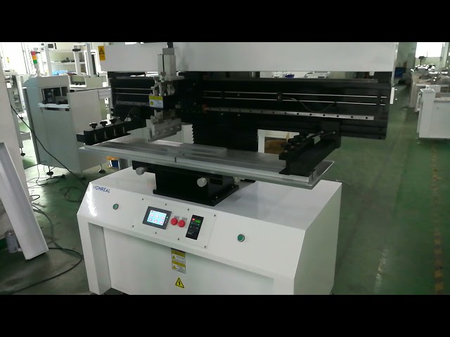
SMT Semi Auto Screen Printer for pcb size 1200 in smt LED production line Product introduction: 1.Using precision guide rail and the import motor to drive the blade seat conversion, printing, and high accuracy. 2.Printing scraper can rotate 45
Training Courses | | | PCB Design Courses
The PCB design courses teach students the process, techniques and tools needed to design layout of printed circuit boards.
SMT Express, Volume 2, Issue No. 3 - from SMTnet.com Volume 2, Issue No. 3 Thursday, March 16, 2000 Featured Article Return to Front Page Stencil Design for Mixed Technology Through-hole / SMT Placement and Reflow by William E. Coleman, Photo
New BGA Solder Mask Repair Technique Using Laser Cut Stencils If you don't see the images, please visit online version at #Application.SmtNet.baseURL#/express/ New BGA Solder Mask Repair Technique Using Laser Cut Stencils Best, Inc
| https://www.feedersupplier.com/sale-13118549-xp142-xp143-xp243-1mm-thickness-fuji-xp-smt-label-feeder.html
XP142 XP143 XP243 1mm Thickness Fuji XP SMT Label Feeder Basic Information Place of Origin: Japan Brand Name: FUJI Model Number: XP142/XP143/XP243 Minimum Order Quantity: 1 unit Price
| http://etasmt.com/cc?ID=te_news_industry,23961&url=_print
Case study: How to Create a Reflow Profile for a 16-layer, 2mm Thickness PCB with a High Density SMT Connector?-SMT Technical-Reflow oven,SMT Reflow Soldering Oven-cmsadmin Reflow oven,SMT Reflow Soldering Oven 当前位置: Home >> News

Products, services, training & consulting for the assembly, rework & repair of electronic assemblies. BGA process experts. Manufacturers Rep, Distributor & Service Provider for Seamark/Zhuomao and Shuttle Star BGA Rework Stations.
Training Provider / Manufacturer's Representative / Equipment Dealer / Broker / Auctions / Consultant / Service Provider
1750 Mitchell Ave.
Oroville, CA USA
Phone: (888) 406-2830


winsouce.jpg)