Industry Directory | Manufacturer
MIRTEC has earned a solid reputation as one of the most Progressive and Dynamic Suppliers of Automated SMT Inspection Equipment to the Electronics Manufacturing Industry.
Industry Directory | Consultant / Service Provider / Manufacturer
Designer & Manufacturer of Acoustic Microscopes for Nondestructive Component Inspection.
ISIS� (Infrared Screening and Inspection Solutions) was developed to detect defects and manufacturing flaws in printed circuit boards (PCBs) that are assembled using surface mount technology (SMT). ISIS� uses infrared imaging and proprietary thermal
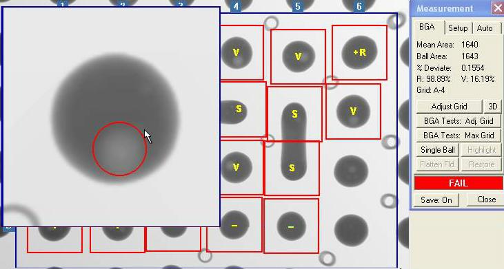
GTI-5000 BGA "Surface Mount" PCB Analysis The GTI-5000 Computer Image Processor is designed for the x-ray analysis of surface mount, BGA and PCB components. The software can provide analysis of BGA defects including bridging, voids and missing ball
Electronics Forum | Sun Aug 09 15:25:17 EDT 2015 | dev88
dear sir i am new for aoi section,my work will be teaching of aoi defect and related to programming, want to know how to make program easily in mirtec 4.1.1 and what are the different standard which we must understand.
Electronics Forum | Tue May 10 09:54:35 EDT 2016 | reinhardk
Hi all, kindly asking for some hint with a problem we encounter with our SPI: After inspection, the SPI should show the defect details, but it doesn't. I can see the files created by the realtime-card in the exchange-directory between windows- and
Used SMT Equipment | AOI / Automated Optical Inspection
Capture on the fly technology 3D Fusion Lighting (RGB+White LED's) 5 megapixel color imaging 2 top-down and 4 side angle cameras Quick set-up High speed, high defect coverage Low false failure rate Programmable conveyor for boards up to 20 x 2
Used SMT Equipment | AOI / Automated Optical Inspection
5 megapixel color imaging / (1) top-down and (4) side angle cameras / quick set-up / high speed / high defect coverage / low false failure rate Complete and Operational USA / FOB Origin Immediate
Industry News | 2003-04-02 09:03:49.0
Configural Recognition(TM) Object and Image-Analysis Technology Enables One-Hour Program Generation
Industry News | 2015-07-06 10:34:12.0
The SMTA announces a new feature area that will debut during the SMTA International Electronics Exhibition: the “SMTA - NPL Solder Paste and Solder Joint Automatic Inspection Experience.” This special feature will take place during both days of the SMTA International Exhibition at the Donald Stephens Convention Center in Rosemont, Illinois on September 29 - 30, 2015.

Parts & Supplies | SPI / Solder Paste Inspection
Quick programming, friendly programming interface Multiple measurement methods True one-button measurement Eight-way motion button, one-click focus Adjustable scanning pitch Solder paste 3D simulation function Powerful SPC function MARK
Parts & Supplies | Soldering Equipment/Fluxes
3D Solder Paste Inspection Machine Features : Easy to use by fully motorize X-Y scan mechanism. Easy to program by Gerber image navigator Easy to repeat the same job by loading the saved program User-friendly color image live view operation Ea
Technical Library | 2013-08-08 15:23:11.0
In this project Machine Vision PCB Inspection System is applied at the first step of manufacturing, i.e., the making of bare PCB. We first compare a PCB standard image with a PCB image, using a simple subtraction algorithm that can highlight the main problem-regions. We have also seen the effect of noise in a PCB image that at what level this method is suitable to detect the faulty image. Our focus is to detect defects on printed circuit boards & to see the effect of noise. Typical defects that can be detected are over etchings (opens), under-etchings (shorts), holes etc...
Technical Library | 2021-05-06 13:48:05.0
In this paper most commonly occurring Bare PCB defects such as Track Cut, Track short and Pad Damages are detected by Image processing techniques. Reference PCB without having any defects is compared with test PCB having defects to identify the defects and x-y coordinates of the center of the defects along with radii are obtained using Difference of Gaussian method and location of the individual type of defects are marked either by similar color or different colors. Result Analysis includes time taken for the inspection of a single defect, multiple similar defects, and multiple different defects. Time taken is ranging from 1.674 to 1.714 seconds if the individual type of defects are marked by different colors and 0.670 to 0.709 seconds if all the identified defects are marked by the same colors.
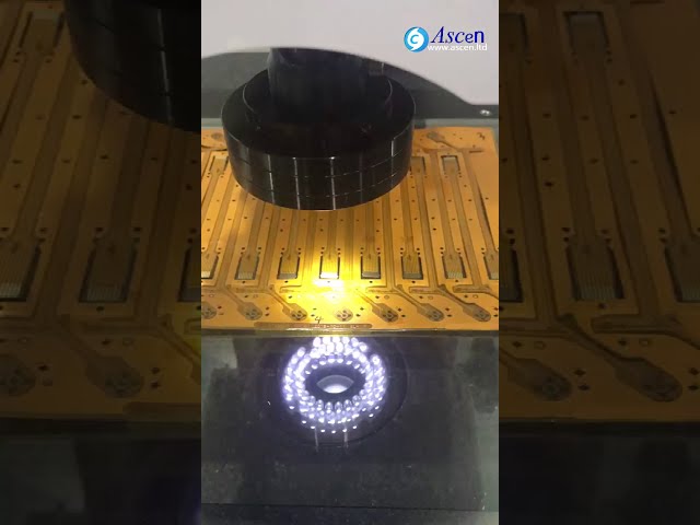
https://www.ascen.ltd/Products/PCB_board_assembly_system/vision_measurin/507.html Vision Measuring Machine and image measuring instrument can be used for dimensional accuracy measurement of various molds, aircraft, automobile, mobile phone, computer,
https://www.ascen.ltd/Products/PCB_board_assembly_system/vision_measurin/507.html Vision Measuring Machine and image measuring instrument can be used for dimensional accuracy measurement of various molds, aircraft, automobile, mobile phone, computer,
Training Courses | | | Other Courses
Other courses related to electronics manufacturing and assembly
Training Courses | | | PCB Assembly Courses
The PCB assembly courses provide knowledge of different processes and equipment used in TH and SMT assembly of printed circuit boards.
Events Calendar | Mon Apr 23 00:00:00 EDT 2018 - Thu Apr 26 00:00:00 EDT 2018 | Shanghai, China
SMTA China East Conference 2018
Events Calendar | Wed Dec 06 00:00:00 EST 2017 - Wed Dec 13 00:00:00 EST 2017 | Rolling Meadows, Illinois USA
X-Ray of PCBs Webtorial
Career Center | Wellsboro, Pennsylvania USA | Engineering
SMT PROCESS ENGINEER: (Wellsboro, PA) - Designs, defines and plans the manufacturing process. Specifies and directs installation of new processes. Plans equipment build schedules and monitors vendor progress. Defines and recommends equipment, methods
Career Center | Milpitas, California USA | Clerical,Production,Quality Control,Research and Development,Technical Support
Winslow Automation, Inc. (aka Six Sigma), an industry leader in electronic component interconnect technology & related test and failure analysis services, is seeking a ‘hands on’ Materials Engineer to join our Test services team. This individual wi
Career Center | seoul, South Korea | Engineering
I have 4 year process engineering in Motorola and 7 years service experience in Assemblen . 2 years in Mirtec AOI as service manager .
Career Center | Grand Prairie, Texas USA | Production,Quality Control,Technical Support
SMT Programmering Specialist. Pick and place, screen printer, AOI and quality inspection, process control, CAD and program development.
SMTnet Express, April 21, 2022, Subscribers: 25,664, Companies: 11,565, Users: 27,188 Deep Learning Based Defect Detection for Solder Joints on Industrial X-Ray Circuit Board Images Quality control is of vital importance during
SMTnet Express August 8, 2013, Subscribers: 26202, Members: Companies: 13446, Users: 35028 Automatic PCB Defect Detection Using Image Substraction Method by Sonal Kaushik, Javed Ashraf; Al-Falah School of Engineering & Technology A printed circuit
| https://www.eptac.com/soldertips/acceptability-of-conformal-coating-bubbles/
. Is Figure 10-131 a Defect Photo? Other than stripping and re-coating , if bubbles are encapsulated would they be considered an acceptable Process Indicator or a Defect? *Image (excerpt
Baja Bid | https://bajabid.com/product/nordson-yestech-bx-benchtop-aoi/
fixture w/ YESClampTM and camera indexing head Full defect coverage at high resolution for PCB’s up to 18” x 20” in size Condition: Complete & Operational Location


