Industry Directory | Consultant / Service Provider
Adhesive Flip Chip Technologies, Bumping Services (Pd, NiAu, polymer...), Assembly Services (Prototyping to High Volume)
New Equipment | Solder Paste Stencils
Laser Fab, NiPlate™, NanoCoat™. NicAlloy-XT™ stencils are the premier laser-cut stencils in the industry. Beginning life as a laser-cut stencil, followed by a secondary process utilizing Photo Stencil’s own proprietary NiPlate™ technology, which fur
Metal Covers are usually Kovar plated with Ni/Au. Covers are sealed to a ceramic or metal package, achieving a hermetic enclosure.
Electronics Forum | Wed Feb 04 06:26:20 EST 2009 | sachu_70
Hi Peter, The defect you observe during the second side reflow could be caused due to improper Au plating thickness in the PCB fabrication process. You can refer IPC-2221 wherein plating thicknes for ENIG mentions 0.08um to 0.23um for Immersion Gold,
Electronics Forum | Tue May 14 22:09:04 EDT 2013 | ultimatejoker
Hi, what is significant different between PdNi and PdCo Plating? I found in some papers indicate that the deposit characteristics for both plating is totally the same.
Used SMT Equipment | Flexible Mounters
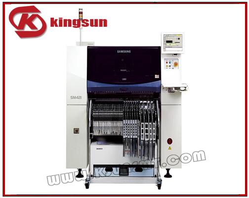
Product Name: Samsung multi-function SM421 chip mounter Product number: SM421 Detailed product introduction Samsung multi function SM421 chip mounter Mounting speed: 21K CPH /QFP (IPC9850) 5.5K CPH Chip (IPC9850) The corresponding components: Ma

Used SMT Equipment | SMT Equipment
Product Name: Samsung multi-function SM421 chip mounter Product number: SM421 Detailed product introduction Samsung multi function SM421 chip mounter Mounting speed: 21K CPH /QFP (IPC9850) 5.5K CPH Chip (IPC9850) The corresponding components: Ma
Industry News | 2020-03-19 13:12:42.0
The SMTA is pleased to announce the Best Papers from SMTA International 2019. As speakers at SMTA International, individuals make contributions to the industry by sharing their research and findings. For these exceptional achievements, a cash award and plaque are given to primary authors of all winning papers.
Industry News | 2016-05-16 20:13:12.0
NEO Tech announces that it will showcase its high-reliability substrate and microelectronic assembly capabilities in booth 2143 at the 2016 IEEE International Microwave Symposium IMS 2016, which is schedule to take place from May 24-26 at the Moscone Center in San Francisco.
Parts & Supplies | Pick and Place/Feeders
ISO 4762 - M 2,5 x 10-10.9,ZiNi plated
.jpg)
Parts & Supplies | Chipshooters / Chip Mounters
700402 SCREW M3X8 CSK.SLTD.M/C ST.ST 700145 SCREW M4X25 CAP HD ST.ST 700118 SCREW M5X25 CAP HD ST.ST 700113 SCREW M4X20 CAP HD ST.ST 700101 SCREW M3X8 CAP HD ST.ST 171321 RETAINER^DIAPH^^340mm LVH 171319 CROSS
Technical Library | 2023-08-04 15:27:30.0
A designed experiment evaluated the influence of several variables on appearance and strength of Pb-free solder joints. Components, with leads finished with nickel-palladium-gold (NiPdAu), were used from Texas Instruments (TI) and two other integrated circuit suppliers. Pb-free solder paste used was tin-silver-copper (SnAgCu) alloy. Variables were printed wiring board (PWB) pad size/stencil aperture (the pad finish was consistent; electrolysis Ni/immersion Au), reflow atmosphere, reflow temperature, Pd thickness in the NiPdAu finish, and thermal aging. Height of solder wetting to component lead sides was measured for both ceramic plate and PWB soldering. A third response was solder joint strength; a "lead pull" test determined the maximum force needed to pull the component lead from the PWB. This paper presents a statistical analysis of the designed experiment. Reflow atmosphere and pad size/stencil aperture have the greatest contribution to the height of lead side wetting. Reflow temperature, palladium thickness, and preconditioning had very little impact on side-wetting height. For lead pull, variance in the data was relatively small and the factors tested had little impact.
Technical Library | 2014-11-06 16:43:24.0
This paper summarizes the results of recent investigations to examine the effect of electroless nickel process variations with respect to Pb-free (Sn-3.0Ag-0.5Cu) solder connections. These investigations included both ENIG and NiPd as surface finishes intended for second level interconnects in BGA applications. Process variations that are suspected to weaken solder joint reliability, including treatment time and pH, were used to achieve differences in nickel layer composition. Immersion gold deposits were also varied, but were directly dependent upon the plated nickel characteristics. In contrast to gold, different electroless palladium thicknesses were independently achieved by treatment time adjustments.
E1378700000 BALL CATCH E1380715000 STICKER E13807260A0 Y AXIS SLIDER ASM E1381726000 LINEAR WAY LWL5 B E1382715000 L STICKER B E1382726000 CHUCK BASE E1383729000 BOARD BASE E1384726000 LM GUIDE RSR92M E13867000A0 HOD BOX ASM

| http://etasmt.com/cc?ID=te_news_industry,3561&url=_print
) and its compounds in some of their manufacturing operations, such as solder plating. This article aims to provide the reader some basic background information on the semiconductor industry's "lead-free" (Pb-free) initiatives
Heller Industries Inc. | https://hellerindustries.com/wp-content/uploads/2022/06/Optimizing-Reflowed-Solder-TIM-sTIMs-Processes-for-Emerging-Heterogeneous.pdf
reference [7], an optimum gold thickness was determined. At the low end, the gaps in the plating resulted in voiding. At the high end, excess IMC growth occurred during reflow and reliability testing. The bondline thickness (BLT) of indium solder preforms is


winsouce.jpg)