Industry News | 2003-06-23 08:49:39.0
Three Organizations from the US, Europe and Japan to
Technical Library | 2015-04-29 03:48:39.0
SPI equipment is routinely used in Printed Circuit Board (PCB) manufacturing to monitor and control one of the most crucial steps affecting the finished quality of circuit board. Solder paste deposition is the key process in board assembly operations using SMT techniques. Our LSM™ system was the industry's first popular method of manually inspecting solder paste; our SE systems revolutionized SMT production by offering an automated method for performing in-process 3D inspection on the assembly line. SPI systems measure the height and volume of the solder pads before the components are applied and the solder melted, and when used properly, can reduce the incidence of solder-related defects to statistically insignificant amounts. Critical to the SPI measurement is the accuracy of the height measurement because that has a direct correlation with solder volume and defects.
Technical Library | 2017-02-28 12:39:50.0
During the last 5 years mobile phones and other portable consumer electronics have been extremely popular and spread all over the world in different climate zones in very high volumes. At the same time the mobile phone terminal for many people has become a necessity that is brought with them in any activity they practice. These changes in user behavior have heavily changed the impact on handheld terminals from moisture, sweat, corrosive atmospheres and mechanical drop. As a result of this the requirement to solder joint reliability, corrosion stability and wear resistance are heavily increasing to keep a high reliability of the terminal.Immersion Ni/Au has been the overall dominant surface finish on Printed Wiring Boards (PWB's) for the last 10 years, but a paradigm shift to avoid use of this thin and porous surface finish is ongoing nowadays because it can’t address these challenges in a satisfactory way.In today's handheld terminals, Organic Solder Preservative (OSP) has replaced Immersion Ni/Au on solder pads. Carbon surface finish for Key- and spring contact-pads, combined with the right concept design can make use of Immersion Ni/Au unnecessary in the near future. The result will be higher reliability with less expensive and simpler processes.This paper will discuss the various considerations for choice of surface finish and results from the feasibility studies performed.
Precision PCB Services, Inc. will like to announce that their new Plano, Texas office is officially open for business. Lan Nguyen O'Donnell, President stated, "that this will allow us to expand our equipment sales and customer support throughout Te
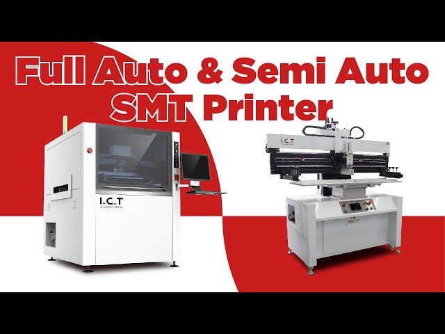
Full-auto SMT Stencil Printer is indispensable equipment in SMT production Line. It is generally composed of board mounting, solder paste, imprinting, and circuit board transfer. Widely used are Full-auto SMT Stencil Printer and semi-auto SMT Stencil
Training Courses | | | PCB Assembly Courses
The PCB assembly courses provide knowledge of different processes and equipment used in TH and SMT assembly of printed circuit boards.
, Nick Munson, Steve Ring, Evan Briscoe.; Foresite In
PCB Libraries, Inc. | https://www.pcblibraries.com/Forum/pad-to-pad-space-in-3pin-sofl_topic2836.html
Pad to Pad space in 3-pin SOFL - PCB Libraries Forum Forum Home > PCB Footprint Expert > Questions & Answers New Posts FAQ Search Events Register Login Pad to Pad space in 3-pin SOFL
| https://www.eptac.com/soldertips/soldertips-issues-with-incomplete-solder-reflow-in-production-2/
: I’m not exactly sure of what you mean by flux exhaustion, however; my interpretation is, there wasn’t enough flux in the solder paste to prepare the pad/land area and have the molten solder flow over the complete pad or land area itself


