New Equipment | Industrial Automation
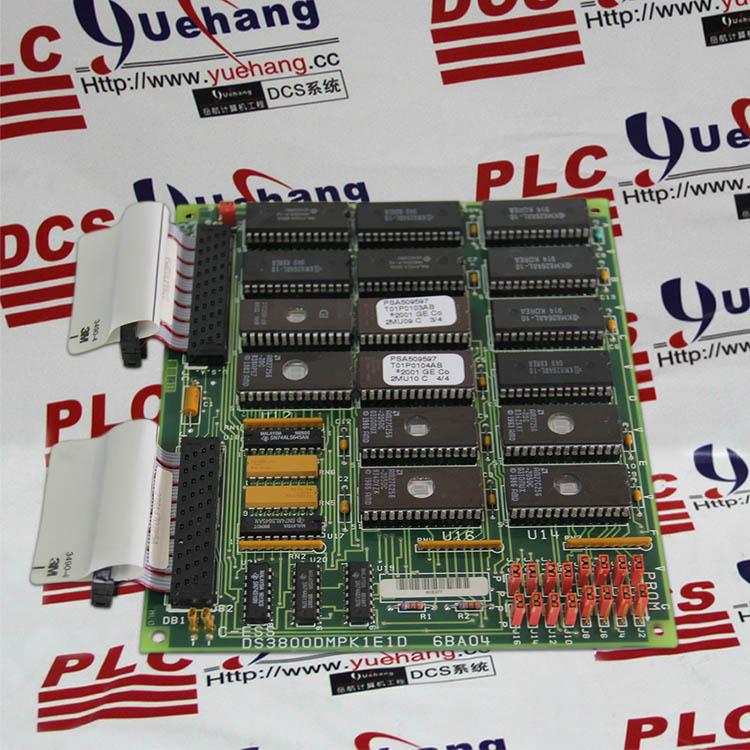
General Electric GIVEN YOUR BEST ! PLEASES mailto:unity@mvme.cn Contact: Sandy Lin Email:unity@mvme.cn Skype:onlywnn_1 Telegram:+8618020776786 Mobile(Whatsapp): (+86)-18020776786 QQ :2851195456 General Electric Company is an Americanmultinati
.jpg)
New Equipment | Industrial Automation
Sandy.[mailto:unity@mvme.cn] Sandy.[WhatsApp/Skype/Mobile:+8618020776786] Sandy.[Quote to you within the shortest possible time with our best price] Warranty: up to 12 months Shipping: fast delivery is available NEW+ORIGINAL+IN STOCK+ONE
Electronics Forum | Thu May 25 15:14:07 EDT 2006 | H
Anyone think that this, http://img336.imageshack.us/my.php?image=nodule27wc.jpg, is a nodule which will eventually grow into a tin whisker? Observe the plating on the component lead. Thanks in advanced for opinions.
Electronics Forum | Thu May 25 15:31:08 EDT 2006 | samir
H, I tried without the commaat the end http://img336.imageshack.us/my.php?image=nodule27wc.jpg Seems to work. IMO, it looks like questionable component plating and not this so-called "nodule".
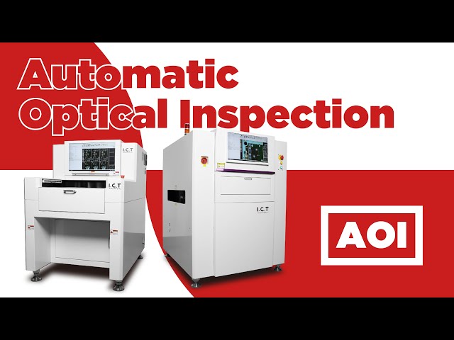
Industry News | 2022-10-12 08:07:17.0
I.C.T Provide SMT Production Line solutions with Automated Optical Inspection (AOI) AOI is short for Automated Optical Inspection, which is widely used in the electronics industry to check the appearance of PCBA assembly at the back end of the circuit board assembly line. The basic principle of AOI is to judge whether the object to be tested meets the standard by comparing whether there is a large difference between the object to be tested and the standard image by using image technology. AOI emits a 4-color light source to the PCBA board, which is automatically scanned by an industrial camera for catastrophic failures, such as missing components or quality defects. Therefore, the quality of AOI depends on the image imaging ability, algorithm parsing ability and image discrimination technology. I.C.T AOI has done well in these aspects.
Industry News | 2013-03-18 11:42:51.0
Last week, in accordance with IPC-A-600, North American bare board manufacturer Saturn Electronics Corporation certified nine Michigan-based employees as IPC Application Specialists.
Technical Library | 2020-08-27 01:22:45.0
Initially adopted internal specifications for acceptance of printed circuit boards (PCBs) used for wire bonding was that there were no nodules or scratches allowed on the wirebond pads when inspected under 20X magnification. The nodules and scratches were not defined by measurable dimensions and were considered to be unacceptable if there was any sign of a visual blemish on wire-bondable features. Analysis of the yield at a PCB manufacturer monitored monthly for over two years indicated that the target yield could not be achieved, and the main reasons for yield loss were due to nodules and scratches on the wirebonding pads. The PCB manufacturer attempted to eliminate nodules and scratches. First, a light-scrubbing step was added after electroless copper plating to remove any co-deposited fine particles that acted as a seed for nodules at the time of copper plating. Then, the electrolytic copper plating tank was emptied, fully cleaned, and filtered to eliminate the possibility of co-deposited particles in the electroplating process. Both actions greatly reduced the density of the nodules but did not fully eliminate them. Even though there was only one nodule on any wire-bonding pad, the board was still considered a reject. To reduce scratches on wirebonding pads, the PCB manufacturer utilized foam trays after routing the boards so that they did not make direct contact with other boards. This action significantly reduced the scratches on wire-bonding pads, even though some isolated scratches still appeared from time to time, which caused the boards to be rejected. Even with these significant improvements, the target yield remained unachievable. Another approach was then taken to consider if wire bonding could be successfully performed over nodules and scratches and if there was a dimensional threshold where wire bonding could be successful. A gold ball bonding process called either stand-off-stitch bonding (SSB) or ball-stitch-on-ball bonding (BSOB) was used to determine the effects of nodules and scratches on wire bonds. The dimension of nodules, including height, and the size of scratches, including width, were measured before wire bonding. Wire bonding was then performed directly on various sizes of nodules and scratches on the bonding pad, and the evaluation of wire bonds was conducted using wire pull tests before and after reliability testing. Based on the results of the wire-bonding evaluation, the internal specification for nodules and scratches for wirebondable PCBs was modified to allow nodules and scratches with a certain height and a width limitation compared to initially adopted internal specifications of no nodules and no scratches. Such an approach resulted in improved yield at the PCB manufacturer.
Technical Library | 2015-11-12 19:04:51.0
In order to provide the functionality in today’s electronics, printed circuit boards are approaching the complexity of semiconductors. For flexible circuits with 1 mil lines and spaces, this means no nodules, no pits, and excellent ductility with thinner deposits. One of the areas that has to change to get to this plateau of technology is acid copper plating. Acid copper systems have changed in minor increments since their introduction decades ago. However, the basic cell design using soluble anodes in slabs or baskets has for the most part remained the same. Soluble, phosphorized, copper anodes introduce particulate and limits the ability to control plating distribution.
I.C.T Provide SMT Production Line solutions with Automated Optical Inspection (AOI) AOI is short for Automated Optical Inspection, which is widely used in the electronics industry to check the appearance of PCBA assembly at the back end of the cir
Training Courses | | | IPC-600 Specialist (CIS)
The Certified IPC-600 Specialist (CIS) training targets quality assurance and acceptance of bare printed circuit boards.
Training Courses | | | IPC-600 Specialist (CIS)
The Certified IPC-600 Specialist (CIS) training targets quality assurance and acceptance of bare printed circuit boards.
Imagineering, Inc. | https://www.pcbnet.com/blog/a-guide-to-pcb-inspection-methods/
. It is particularly useful for detecting issues early in printed circuit board manufacturing, such as scratches, nodules, stains, thinning solder, open circuits, and short circuits
| https://www.smtfactory.com/I-C-T-Automated-Optical-Inspection-AOI-to-Improve-SMT-Line-Efficiency-id43297267.html
? AOI can be used to detect many surface defects, including scratches, nodules, stains, open, short circuits, inadequate or excessive solder, incorrect components, missing components, faulty polarity of components, etc. smt aoi machine aoi machine SMT aoi


