Industry Directory | Consultant / Service Provider / Manufacturer
Tropical Stencil is dedicated to providing the highest quality Laser Cut Stencils; with our rapid response, you will have your Stencil delivered on-time.
New Equipment | Solder Materials
8 hours), and abandon time (>4 hours) Printing: Suitable for high speed printing up to 150 mm/s Reflow: Solderable on challenging surface finishes (CuNiZn and Copper OSP) Colorless residues for easy post-reflow inspection Careful contr

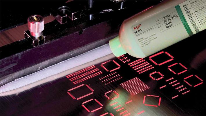
New Equipment | Solder Materials
As the world's leading developer of advanced solder paste materials, Henkel delivers decades of technology and expertise for optimized process performance. With ground breaking new formulations to provide an easy transition to lead-free as well as pr
Electronics Forum | Thu May 25 11:51:12 EDT 2000 | AF Ng
Hi,Wolfgang Busko, Thank you for your help. Still need some advice. If the OSP board having stencil rest on the solder mask, then, would it has more gasketing effect( solder paste squeezed out to the underside of the stencil), as compared to the HAS
Electronics Forum | Wed May 24 11:35:15 EDT 2000 | Bill Ng
Could someone help to let me know when we are doing stencil printing of solder paste on board with OSP surface finish on the land, the stencil is resting on the solder mask or the land itself. If it is resting on the solder mask, then, the actual pas
Industry News | 2013-08-07 09:58:46.0
The SMTA launched an online re-certification program for engineers whose 10-year SMT Processes Certification is expiring.
Industry News | 2018-10-18 08:55:30.0
Nitrogen Protection Reflow Oven
Events Calendar | Tue Apr 13 00:00:00 EDT 2021 - Tue Apr 13 00:00:00 EDT 2021 | ,
Boston Chapter Webinar: Cleaning Chemistry For PWB and Rework - Part 2, session 1
Events Calendar | Tue Apr 13 00:00:00 EDT 2021 - Tue Apr 13 00:00:00 EDT 2021 | ,
Boston Chapter Webinar: Cleaning Chemistry For PWB and Rework - Part 2, session 2
Career Center | Rochester, New York USA | Engineering
I have done my undergraduate studies in Mechanical Engineering. I am pursuing my Master's Program in Electronics Packaging. I am currently working as a Research Assistant for RIT-CEMA (Center for Electronics Manufacturing and Assembly). My research
Career Center | Phoenix, Arizona | Engineering,Management,Production,Quality Control,Research and Development,Sales/Marketing,Technical Support
• Highly motivated, solution oriented professional with proven record synergizing scientific, engineering, and business administration backgrounds to drive and sustain customer satisfaction and long term improvements. • Articulate communicator that a
Heller Industries Inc. | https://hellerindustries.com/wp-content/uploads/2018/07/pan_APEX06.pdf
% Sn finish OSP over Cu pad Sn63Pb37, Type 3 powder, No-clean flux 1206, 0805, 0603, 0402 all 100% Sn finish HASL SnPb over Cu pad The test vehicle designed is shown in Figure 1
Imagineering, Inc. | https://www.pcbnet.com/blog/how-pcbs-are-made/
: A layer of photosensitive material, called photoresist, is applied to the substrate. A mask—similar to a stencil—is placed over the PCB


.gif)


