The PCB Footprint Expert is a powerful CAD library development tool powered by our own proprietary CAD LEAP Technology (Libraries Enhanced with Automated Preferences). It is packed with very powerful advanced library management features that cuts foo
New Equipment | Test Equipment
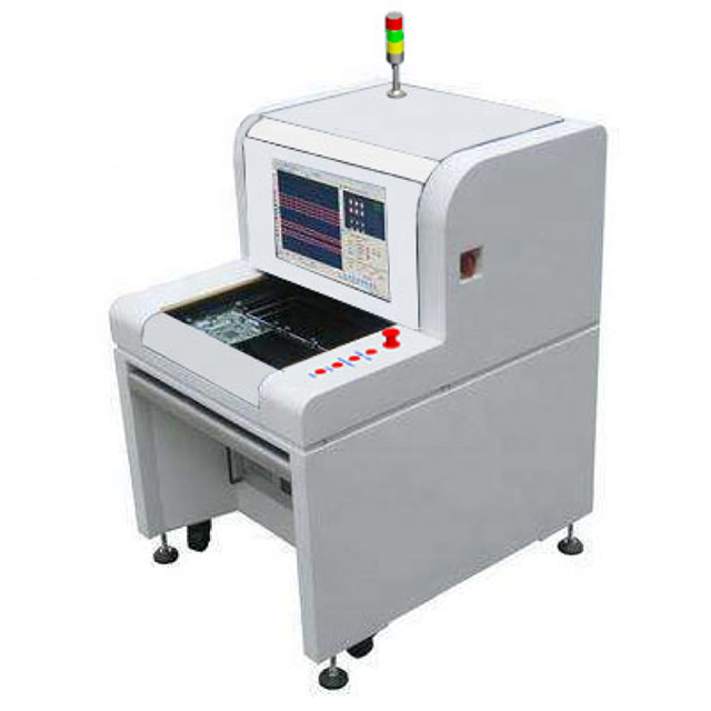
RISON Offline Automatic Optical -AOI-50 Leading the Way for Inspection Solutions RX-AOI50 is an offline AOI specially developed for many manufacturers making several different machines in limited quantities. Imported screw guides achieve the h
Industry News | 2024-03-18 12:29:00.0
Impossible Objects proudly announces plans to exhibit at Apex 2024, scheduled to take place April, 9-11, 2024 at Anaheim Convention Center. The focus of this exhibition is the game-changing CBAM-25 industrial 3D printer, a true paradigm shift in high-speed, high-performance additive manufacturing.
Industry News | 2025-09-24 21:25:38.0
By Teh-Kuang‑ Lung, President and CEO, Naprotek, LLC

The PCB Footprint Expert is a powerful CAD library development tool powered by our own proprietary CAD LEAP Technology (Libraries Enhanced with Automated Preferences). It is packed with very powerful advanced library management features that cuts foo
Surface Mount Technology Association (SMTA) | https://www.smta.org/news/smta_calendar/calendar.cfm
design completion. All these issues play a part of the design, manufacturing and performance of our end products. Attendees will receive an understanding of how to create good design-data, allowing for manufacturing tolerance allowances . The goal is to
ASYMTEK Products | Nordson Electronics Solutions | https://www.nordson.com/en/divisions/efd/resources/solder-dictionary-of-terms
). F Fillet Solder formation at the intersection of surfaces of a solder connection. Fine Pitch Centerline spacing of leads 0.5 mm (20 mils) or less. Flux A material that cleans metal surfaces of absorbed gases, oxide films, and other surface contaminants