Industry Directory | Manufacturer
PCB Repairs of all kinds including-Solder on Tab (Solder Removal, Gold Plating), PTH & Delam repairs, etc.
Industry Directory | Manufacturer
PWB designs and manufactures test equipment and provides services to test the reliability of Printed Circuit Boards.
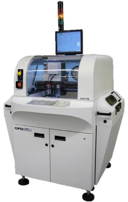
Precision Dispensing System for Heated Dispense Applications The GPD Global MAX II is a compact; high-accuracy system designed for today’s advanced heated dispensing applications. The frame is molded from “liquid rock” which gives the system a stabl
New Equipment | Education/Training
This specification covers qualification and performance of rigid PCBs including with or without plated-through holes, single-sided, double-sided, multilayer with or without blind/buried vias and metal core boards. It addresses final finish and surfac
Electronics Forum | Thu Oct 31 02:43:55 EDT 2013 | hqew2013
The smallest finished hole available for 2 layer board is .020”. The smallest finished hole available for 4+ layer board is .014”. All holes are round and drilled through from top to bottom layer of board. No blind or buried vias. For holes = .15
Electronics Forum | Mon Feb 26 20:02:42 EST 2001 | davef
First, I don�t understand why your board fabricator can�t do a good job plugging your vias. Additionally, when you consider that they forgot to plug the first batch of boards, it makes me wonder if they are desirable as a supplier. Generally, we us
Technical Library | 2019-06-26 23:21:49.0
Copper-filled micro-vias are a key technology in high density interconnect (HDI) designs that have enabled increasing miniaturization and densification of printed circuit boards for the next generation of electronic products. Compared with standard plated through holes (PTHs) copper filled vias provide greater design flexibility, improved signal performance, and can potentially help reduce layer count, thus reducing cost. Considering these advantages, there are strong incentives to optimize the via filling process. This paper presents an innovative DC acid copper via fill formulation, for VCP (Vertical Continues Plating) applications which rapidly fills vias while minimizing surface plating.
Technical Library | 2019-07-17 17:56:34.0
The increased demand for electronic devices in recent years has led to an extensive research in the field to meet the requirements of the industry. Electrolytic copper has been an important technology in the fabrication of PCBs and semiconductors. Aqueous sulfuric acid baths are explored for filling or building up with copper structures like blind micro vias (BMV), trenches, through holes (TH), and pillar bumps. As circuit miniaturization continues, developing a process that simultaneously fills vias and plates TH with various sizes and aspect ratios, while minimizing the surface copper thickness is critical. Filling BMV and plating TH at the same time, presents great difficulties for the PCB manufactures. The conventional copper plating processes that provide good via fill and leveling of the deposit tend to worsen the throwing power (TP) of the electroplating bath. TP is defined as the ratio of the deposit copper thickness in the center of the through hole to its thickness at the surface. In this paper an optimization of recently developed innovative, one step acid copper plating technology for filling vias with a minimal surface thickness and plating through holes is presented.
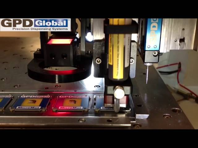
Precision Dispensing System for Heated Dispense Applications The GPD Global MAX II is a compact; high-accuracy system designed for today’s advanced heated dispensing applications. The frame is molded from “liquid rock” which gives the system a stabl

Teaching video on PCB through hole repair. BEST instructors teach the method for repair of a damaged eyelet using a multitude of different close up and angled views. Repair is completed per the IPC 7721 instructions. http://www.solder.net
Training Courses | | | IPC-6012 Specialist (CIS)
The Certified IPC-6012 Specialist (CIS) training covers design, fabrication and inspection of rigid printed boards.
Training Courses | | | IPC-6012 Trainer (CIT)
The Certified IPC-6012 Trainer (CIT) courses recognize individuals as qualified trainers in the area of design, fabrication and inspection of rigid printed boards and prepare them to deliver Certified IPC-6012 Specialist (CIS) training.
Career Center | Lalkua, India | Engineering,Maintenance,Production,Quality Control,Research and Development,Technical Support
Machine maintenance Service and support knowledge with customer satisfactory. Deal with customers at all level via phone,remote and mail.Sound knowledge of PCB fabrication machine.
SMT Express, Volume 2, Issue No. 3 - from SMTnet.com Volume 2, Issue No. 3 Thursday, March 16, 2000 Featured Article Return to Front Page Stencil Design for Mixed Technology Through-hole / SMT Placement and Reflow by William E. Coleman, Photo
SMTnet Express, July 18, 2019, Subscribers: 32,162, Companies: 10,836, Users: 24,951 Via Fill and Through Hole Plating Process with Enhanced TH Microdistribution Credits: MacDermid Inc. The increased demand for electronic devices in recent years
PCB Libraries, Inc. | https://www.pcblibraries.com/Forum/proportional-throughhole-padstacks_topic90_post41.html
Nick B Report Post Thanks(0) Quote Reply Posted: 20 Mar 2012 at 2:40am The link above was updated again: Updated the Thermal Spoke Width calculations for Plated Through Hole padstacks The new improved formula is: Spoke Width = 75
ASYMTEK Products | Nordson Electronics Solutions | https://www.nordson.com/en/divisions/dage/application/smt
. This is particularly important if your boards feature BGA devices, QFNs, plated through holes or PTH through hole components. Ruby XL allows inspection of large backplane boards used in servers and for 5G


