Industry Directory | Manufacturer
Manufacture high-density memory and processor-based products, displays, interfaces
Industry Directory | Manufacturer
3M's Electronic Solutions Division designs, manufactures and markets a wide variety of electronic interconnect and protection products.
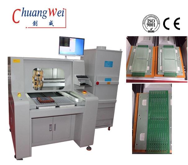
PWB Depaneling Machine Automatic CNC PCB Separator Equipment PCB Separator also called PWB Depaneling machine . Rotate router bit to cut high-density component PCB panel to single products v-groove or perforated line . Utilize all of our accumulat

PCB Separator also called PWB Depaneling machine . Rotate router bit to cut high-density component PCB panel to single products v-groove or perforated line . Utilize all of our accumulated technology to help minimize dust attach on PCB . Router machi
Electronics Forum | Sat Feb 18 09:20:09 EST 2012 | davef
The 3-Tier PCB library concept was originally created by IEC (International Electromechanical Commission) in 1999 and introduced to IPC in 2000. The concept had to be created as a solution for high density packaging for hand held devices to ruggedize
Electronics Forum | Mon Mar 21 12:02:09 EST 2005 | Rob
Hi Colin, Are you using the 1206 package with 4 elements or one of the higher density smaller packages? With the first type you can get them in both Convex or Concave terminations, with most of the solderability problems associated with using the C
Used SMT Equipment | In-Circuit Testers
Agilent HP 3070 In Circuit Test System For Sale The system came off line in good running condition! Machine is complete with keyboard, mouse, and all cable connections Please see attached pictures and configuration below copied from file !!!! 5 0 2 1

Used SMT Equipment | X-Ray Inspection
Make: Glenbrook Model: Jewel Box 90T Year: 2016 Type: X-Ray Inspection Details: The Glenbrook JewelBox 90T is a high-resolution, real-time X-ray inspection system designed for precision i
Industry News | 2013-08-15 20:58:22.0
Heller Industries announced today that they have entered into a joint development agreement with International Business Machines Corporation (NYSE: IBM), to collaborate on the development of fluxless mass reflow furnace equipment and process for high volume manufacturing. The fluxless process utilizes gas phase formic acid to replace standard fluxing agents, and eliminates the need for pre-reflow fluxing and post-reflow flux cleanup steps.
Industry News | 2003-02-25 08:18:29.0
Teradyne can now provide deep micro-via technology for customers of high-performance printed circuits.

Parts & Supplies | Pick and Place/Feeders
The definition of SMT SMT is the surface assembly technology,surface mount technology(surface mount technology)(Surface Mounted Technology abbreviation),is currently the most popular electronic assembly industry,a technology and technology. What a
Technical Library | 2023-01-17 17:58:36.0
Heterogeneous integration has become an important performance enabler as high-performance computing (HPC) demands continue to rise. The focus to enable heterogeneous integration scaling is to push interconnect density limit with increased bandwidth and improved power efficiency. Many different advanced packaging architectures have been deployed to increase I/O wire / area density for higher data bandwidth requirements, and to enable more effective die disaggregation. Embedded Multi-die Interconnect Bridge (EMIB) technology is an advanced, cost-effective approach to in-package high density interconnect of heterogeneous chips, providing high density I/O, and controlled electrical interconnect paths between multiple dice in a package. In emerging architectures, it is required to scale down the EMIB die bump pitch in order to further increase the die-to-die (D2D) communication bandwidth. Aa a result, bump pitch scaling poses significant challenges in the plated solder bump reflow process, e.g., bump height / coplanarity control, solder wicking control, and bump void control. It's crucial to ensure a high-quality solder bump reflow process to meet the final product reliability requirements. In this paper, a combined formic acid based fluxless and vacuum assisted reflow process is developed for fine pitch plated solder bumping application. A high-volume production (HVM) ready tool has been developed for this process.
Technical Library | 2015-08-27 15:32:16.0
Ever since there has been a widespread usage of surface mount parts, the trend of continued shrinkage of devices with ever finer pitches has continued to challenge PCB assemblers for the rework of same. Todays' pitches are commonly 0.5 to 0.4mm with packages of tiny outline sizes, 5 -10mm square, making the rework of such devices a challenge. In addition to the handling and inspection challenges comes the board density. Spacing to neighboring components continues to be compressed so the rework techniques should not damage neighboring components.

ACI Technologies Inc. (ACI) is a scientific research corporation dedicated to the advancement of electronics manufacturing processes and materials for The Department of Defense and industry. This video provides an overview of our commercial service

Hear what attendees had to say about the Electronics in Harsh Environments Conference. Start planning your participation for the 2020 event: 21-23 April 2020 | Amsterdam, Netherlands https://www.smta.org/harsh
Training Courses | | | PCB Design Courses
The PCB design courses teach students the process, techniques and tools needed to design layout of printed circuit boards.
Events Calendar | Tue Jul 17 00:00:00 EDT 2018 - Wed Jul 18 00:00:00 EDT 2018 | ,
Fan Out Packaging- Technology Overview and Evolution - SMTA Webtorial
Events Calendar | Tue Sep 08 00:00:00 EDT 2020 - Tue Sep 08 00:00:00 EDT 2020 | ,
Post – Moore's Law Electronics: From Now until Quantum Computing
Career Center | Fremont, California USA | Engineering
Interprets electrical design requirements and uses Allegro design tool to create original PCB layouts, detailed fab drawings, schematics, and other design files. Work with HW design engineer to make sure PCB layout meet PCB design requirements.
Career Center | Fremont, California USA | Engineering
Job Description: • Has full ownership of HW design and release including HW specification creation, schematic generation, PCB layout, board bring up, and design verification. • Complete PCB design schematic using Orcad capture. • Complete HW desig
Career Center | GOBICHETTIPALAYAM, India | Engineering
PCB design, layout and packaging of high-speed, high-density, Mixed Technology Analog / Digital signals & RF signals, Flex, Rigid board, Commercial, Application Boards, based on client requirement and Quality Inspection of the design.
SMTnet Express, March 1, 2018, Subscribers: 31,280, Companies: 10,908, Users: 24,452 Deposition of Solder Paste into High Density Cavity Assemblies Fernando Coma, Jeffrey Kennedy, Thilo Sack; Celestica Corporation Circuit functional density
Heller Industries Inc. | https://hellerindustries.com/wp-content/uploads/2022/06/Vacuum-Fluxless-Reflow-Technology-for-Fine-Pitch.pdf
. Many different advanced packaging architectures have been deployed to increase I/O wire / area density for higher data bandwidth requirements, and to enable more effective die disaggregation
Surface Mount Technology Association (SMTA) | https://www.smta.org/icsr/call_for_papers.cfm
& regulations Interconnects & component packaging: Alternative interconnects Nano-interconnects High density interconnects Package-on-package Substrates


