Industry Directory | Consultant / Service Provider
PCB assembly services, both US and offshore. We handle basic through-hole to standard surface mount to ultra-fine pitch. Quote and order PCB fabrication and assembly online.
Industry Directory | Manufacturer
Shenzhen Huancheng Automation equipment Co.,ltd (referred to as the "HC"), a High-speed developing enterprise specializing in High Precision Automatic Solder Paste Printer research and development.
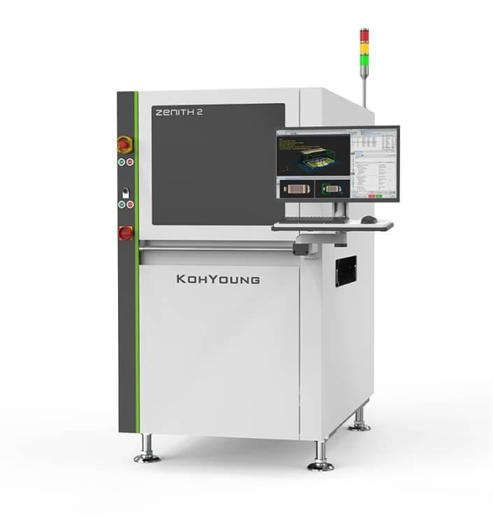
New Equipment | Test Equipment
KOH YOUNG ZENITH 2 3D AOI 8 directional projection light system Camera resolution: 8M 15μm maximum Height measurement: 10 mm Max PCB 490 x 510 mm weight: 600kg Dimension: 1000x1295x1627 mm KOH YOUNG ZENITH 2 3D AOI KOH YOUNG ZENITH 2 3D AOI R

Product Description: The Laser Depaneling Machine is an innovative online or offline PCB laser depaneling equipment with extraordinary cut quality holding tolerances down to as small as 50 microns. It features a powerful Optowave laser with a wavele
Electronics Forum | Thu Dec 05 02:15:12 EST 2019 | sssamw
IPC 2221B mentions a minimum clearance of 0.5 mm between adjacent holes. A drill-to-drill spacing of 20 mils is a standard value in manufacturer design rules. For small annular rings and pad-to-pad clearance, the minimum via distance is often defin
Electronics Forum | Tue Nov 23 23:42:34 EST 1999 | armin
Is there a Standard/Guidelines that (or which IPC guidelines) defines the pad edge-pad edge clearance for Various via hole and component land sizes. Also defining why Vias shouldn't be placed under discrete components.

Used SMT Equipment | Screen Printers
Substrate processing: Maximum substrate size (XxY): 609.6mmx508mm(24”x20”) For circuit boards larger than 20”, special fixtures are required Minimum substrate size (XxY): 50.8mmx50.8mm(2”x2”)
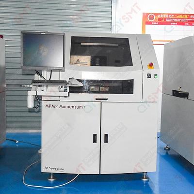
Used SMT Equipment | Screen Printers
Momentum was designed and built to be a no-nonsense production machine. Cost-efficient and featuring a modest footprint, it grows with the user; innovative patented features can be added on or retrofitted as needed as the user’s throughput dema
Industry News | 2018-10-18 08:32:52.0
How to Prevent Solder Ball and Bridging Defects during the SMT Reflow Process
Industry News | 2012-04-09 13:45:59.0
As the electronics assembly industry evolves, printed circuit board (PCB) features and surface mount technology (SMT) components continue to get smaller and smaller. This miniaturization shrinks the process window at print, placement, and reflow, increasing the opportunities for defects.
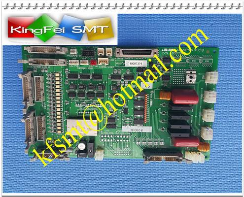
Parts & Supplies | Assembly Accessories
Detailed Product Description Brand: JUKI Part Name: Conveyor PCB Part Number: 40007373 40007374 Machine: FX1R,2050 Condition: Original Used Origin: Japan 40007374 JUKI Conveyor PCB For FX1R Surface Mounting Machine P/N 40007373 Original Part
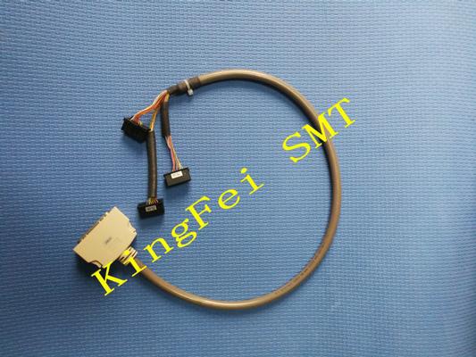
Parts & Supplies | Assembly Accessories
Detailed Product Description Part Name: LNC60 I/F Cable ASM Part Number: 40070445 Machine: JUKI KE2070 2080 FX3 Machine Condition: Original New Brand: JUKI Application: For LNC60 Laser 40070445 LNC60 I/F Cable ASM(2012) For JUKI 2070 2080 FX3 Mac
Technical Library | 2023-05-02 19:03:34.0
The demand for 0201 components in consumer products will increase sharply over the next few years due to the need for miniaturization. It is predicted that over 20 billion 0201 components will be used in more than one billion cell phones worldwide by the year 2003. Therefore, research and development on 0201 assembly is becoming a very hot topic. The first step to achieve a successful assembly process is to obtain a good PCB design for 0201 packages. This paper presents the data and criteria of PCB design for 0201 packages, including the pad design for 0201 components, and the minimum pad spacing or component clearance between 0201 components or between 0201 and other components. A systematic study on pad design and pad spacing was undertaken, using two test vehicles and three Design of Experiments (DOEs). In the first DOE, 2 out of 18 types of 0201 pad designs were selected based on process yield. The second DOE was focused on pad spacing, including 10mil, 8mil, 6mil and 4mil. The third experiment was final optimization, using two types of optimized pad designs with 10mil, 8mil and 6mil pad spacing. Through the above experiments, the design guideline for PCB layout for 0201 packages and the assembly process capability are identified.
Substrate processing: Maximum substrate size (XxY): 609.6mmx508mm(24”x20”) For circuit boards larger than 20”, special fixtures are required Minimum substrate size (XxY): 50.8mmx50.8mm(2”x2”)
Momentum was designed and built to be a no-nonsense production machine. Cost-efficient and featuring a modest footprint, it grows with the user; innovative patented features can be added on or retrofitted as needed as the user’s throughput dema
| https://pcbasupplies.com/replacement-brass-pad-pack-of-10/
Replacement Brass Pad, Pack of 10 Login Create Account Contact View My Cart Menu × Categories Hand Soldering & Rework Automation Tooling PCB Support Systems Soldering Robots Material Handling Dry Storage Cabinets Component Handling Selective Solder Nozzles Pick
| https://www.eptac.com/faqs/ask-helena-leo/ask/smt-components-during-reflow-float-off-pads
(adequate side joint length, not violating minimum electrical clearance, etc.). The IPC does not stipulate that the heel needs to be on pad


