
Industry Directory | Consultant / Service Provider / Media / Publisher / Online Resource / Other
PCB Libraries' "Footprint Expert" suite uses CAD LEAP(tm) Technology to greatly simplify footprint and 3D STEP model creation; it is used by tens of thousands of PCB designers and engineers all over the world.
New Equipment | Fabrication Services
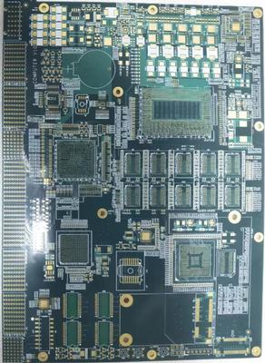
HDI PCB Manufacturer & Assembly – One-stop services from China -HDI (high-density interconnection board) is a compact circuit board designed for small capacity users. Compared with ordinary PCB, the most significant feature of HDI is that the wiri
New Equipment | Rework & Repair Services
MLT provides laser rework services for PCB's including pad / component isolation and trace cutting. Contacts, pads, or other metal features can be laser defined or redimensioned without plunging into the dielectrics below. Trace cuts can be on the
Electronics Forum | Wed Dec 08 19:50:34 EST 2004 | shen_zte
can anyone tell me the benifit of the solder mask onto pad(part) or pad defined by solder mask?and how to excute the SMT process ? thanks.
Electronics Forum | Fri Dec 10 08:42:37 EST 2004 | mattkehoe
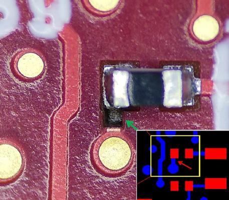
We had some bad experiences trying to work with soldermask defined BGA pads. If the opening in the soldermask is right to the edge of the copper/pad without a space it can leave reside on the pad and nothing will stick to it. See http://www.sipad.com
Industry News | 2017-05-11 17:06:16.0
Library Expert Lite automatically builds footprints and 3D STEP models for tens of millions of parts, for free.
Industry News | 2018-02-01 02:56:53.0
More is not less, rather more is completely free. These newly released features were originally available to our enterprise-level customers, and now available at absolutely no cost, no obligation, no strings attached, to automate creation of tens of millions of parts...
Technical Library | 2008-04-08 17:42:27.0
Concern about the failure of lead-free BGA packages when portable devices such as cell phones are accidentally dropped and a general concern about the resistance of these packages under shock loading has prompted an interest in the impact strength of the soldered BGA connection. This paper reports the results of the measurement of the impact strength of lead-free 0.5±0.01mm diameter BGA spheres on 0.42mm solder mask defined pads on copper/OSP and ENIG substrates using recently developed equipment that can load individual BGA spheres at high strain rates in shear and tension.
Technical Library | 2020-08-27 01:22:45.0
Initially adopted internal specifications for acceptance of printed circuit boards (PCBs) used for wire bonding was that there were no nodules or scratches allowed on the wirebond pads when inspected under 20X magnification. The nodules and scratches were not defined by measurable dimensions and were considered to be unacceptable if there was any sign of a visual blemish on wire-bondable features. Analysis of the yield at a PCB manufacturer monitored monthly for over two years indicated that the target yield could not be achieved, and the main reasons for yield loss were due to nodules and scratches on the wirebonding pads. The PCB manufacturer attempted to eliminate nodules and scratches. First, a light-scrubbing step was added after electroless copper plating to remove any co-deposited fine particles that acted as a seed for nodules at the time of copper plating. Then, the electrolytic copper plating tank was emptied, fully cleaned, and filtered to eliminate the possibility of co-deposited particles in the electroplating process. Both actions greatly reduced the density of the nodules but did not fully eliminate them. Even though there was only one nodule on any wire-bonding pad, the board was still considered a reject. To reduce scratches on wirebonding pads, the PCB manufacturer utilized foam trays after routing the boards so that they did not make direct contact with other boards. This action significantly reduced the scratches on wire-bonding pads, even though some isolated scratches still appeared from time to time, which caused the boards to be rejected. Even with these significant improvements, the target yield remained unachievable. Another approach was then taken to consider if wire bonding could be successfully performed over nodules and scratches and if there was a dimensional threshold where wire bonding could be successful. A gold ball bonding process called either stand-off-stitch bonding (SSB) or ball-stitch-on-ball bonding (BSOB) was used to determine the effects of nodules and scratches on wire bonds. The dimension of nodules, including height, and the size of scratches, including width, were measured before wire bonding. Wire bonding was then performed directly on various sizes of nodules and scratches on the bonding pad, and the evaluation of wire bonds was conducted using wire pull tests before and after reliability testing. Based on the results of the wire-bonding evaluation, the internal specification for nodules and scratches for wirebondable PCBs was modified to allow nodules and scratches with a certain height and a width limitation compared to initially adopted internal specifications of no nodules and no scratches. Such an approach resulted in improved yield at the PCB manufacturer.
PI is so simple. Anyone can use it : automatic programming, no fine-tuning, no keyboard, no mouse, .... PI delivers full 3D and 2D images over the entire board of a size and quality never reached until today. You will see your print process like neve
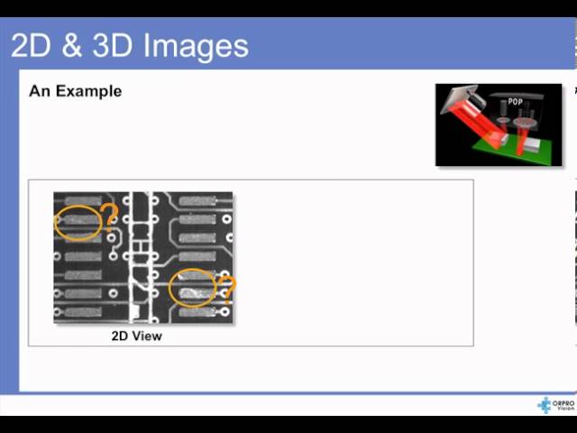
ORPRO Vision SPI Presentation. This presentation introduces the methods and technology used by ORPRO Vision in the Symbion P36 Plus SPI system. For additional information, please contact ORPRO Vision at sales.us@orprovision.com sales.eu@orprovision
Career Center | Wellsboro, Pennsylvania USA | Engineering
SMT PROCESS ENGINEER: (Wellsboro, PA) - Designs, defines and plans the manufacturing process. Specifies and directs installation of new processes. Plans equipment build schedules and monitors vendor progress. Defines and recommends equipment, methods
| https://www.eptac.com/wp-content/uploads/2013/08/eptac_08_21_13-1.pdf
ORION Industries | http://orionindustries.com/pdfs/PDS_GPVOS_0305E.pdf
carrier.The material can be used as an interface where one side is in contact with a leaded device. Note: Resultant thickness is defined as the final gap thickness of the application. Gap Pad VO Soft®


.gif)


