Industry Directory | Other / Consultant / Service Provider / Media / Publisher / Online Resource
PCB Libraries' "Footprint Expert" suite uses CAD LEAP(tm) Technology to greatly simplify footprint and 3D STEP model creation; it is used by tens of thousands of PCB designers and engineers all over the world.

Industry Directory | Other / Consultant / Service Provider / Manufacturer
ScanCAD is an industry leader in inspection, measurement, process control and reverse engineering. Our solutions support OEM's, manufacturers, stencil fabricators, repair depots, and others in optimizing quality and yield.
New Equipment | Rework & Repair Equipment
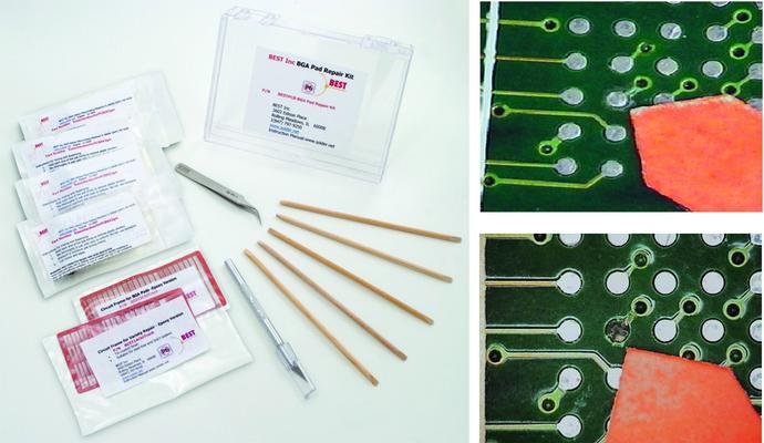
The BEST PCB pad repair repair kit gives you the tools you need for fast modification and repair of PCB circuit pads-no matter what their size. Our online PCB repair training videos, our master instructors along with these materials allows you to mee

New Equipment | Rework & Repair Equipment
The BEST PCB Epoxy Repair Kit can be used to repair lifted pads and traces as well as build up and repair edge corner damage to PCBs or repair solder mask which has been damaged or removed. By adding colorants a pcb color epoxy kit can be made up cus
Electronics Forum | Thu Feb 12 20:42:10 UTC 2026 | SMTA-64387381
Is there any good reason not to print solder paste on DNPs on ENIG plated PCBs? Want to use a single stencil for building several BOM configurations on a common PCB. The in house design team is saying they do not allow printing on the DNP pads.
Used SMT Equipment | Pick and Place/Feeders
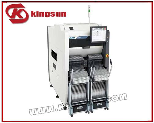
Product number: RX - 7 Detailed product introduction Characteristic With high productivity, versatility, highquality new modular placement machine RX 7 listed Component placement speed (best conditions): 75000 CPH chip components Element size: 0

Used SMT Equipment | SMT Equipment
Product name: RX 7 high-speed module chip mounter Product number: RX - 7 Detailed product introduction Characteristic With high productivity, versatility, high quality new modular placement machine RX 7 listed Component placement speed (best con
Industry News | 2003-06-17 08:07:40.0
The Radiall SMT coupler range now includes the new 14.2 x 5.1mm mini type.
Industry News | 2009-10-17 09:43:47.0
Reduce PCB Repair Costs
Technical Library | 2023-05-02 19:06:43.0
As 0402 has become a common package for printed circuit board (PCB) assembly, research and development on mounting 0201 components is emerging as an important topic in the field of surface mount technology for PWB miniaturization. In this study, a test vehicle for 0201 packages was designed to investigate board design and assembly issues. Design of Experiment (DOE) was utilized, using the test vehicle, to explore the influence of key parameters in pad design, printing, pick-andplace, and reflow on the assembly process. These key parameters include printing parameters, mounting height or placement pressure, reflow ramping rate, soak time and peak temperature. The pad designs consist of rectangular pad shape, round pad shape and home-based pad shape. For each pad design, several different aperture openings on the stencil were included. The performance parameters from this experiment include solder paste height, solder paste volume and the number of post-reflow defects. By analyzing the DOE results, optimized pad designs and assembly process parameters were determined.
Technical Library | 2015-05-28 17:34:48.0
The printed circuit board assembly industry has long embraced the "Smaller, Lighter, Faster" mantra for electronic devices, especially in our ubiquitous mobile devices. As manufacturers increase smart phone functionality and capability, designers must adopt smaller components to facilitate high-density packaging. Measuring over 40% smaller than today's 0402M (0.4mmx0.2mm) microchip, the new 03015M (0.3mm×0.15mm) microchip epitomizes the bleeding-edge of surface mount component miniaturization. This presentation will explore board and component trends, and then delve into three critical areas for successful 03015M adoption: placement equipment, assembly materials, and process controls. Beyond machine requirements, the importance of taping specifications, component shape, solder fillet, spacing gap, and stencil design are explored. We will also examine how Adaptive Process Control can increase production yields and reduce defects by placing components to solder position rather than pad. Understanding the process considerations for 03015M component mounting today will help designers and manufacturers transition to successful placement tomorrow.

PCB pad repair technique demonstrated using the 2-part epoxy method. More on this PCB pad repair technique: http://www.solder.net/services/pcb-repair/pad-and-trace-repair/ More on the recommended epoxy: http://www.soldertools.net/pcb-repair-epoxy-r

This video is on the dry film pad repair technique per IPC 7721 standards. BEST professional instructors demonstrate the proper technique for the repair for PCB pads using the dry film. http://www.solder.net More on PCB pad repair here: http://www.s
Training Courses | | | PCB Rework and Hand Soldering Courses
The PCB rework and hand soldering courses courses cover techniques of rework and repair of PCBs, BGAs and other electronics assemblies, and teach fundamentals of soldering of electronics assemblies.
Training Courses | | | PCB Rework and Hand Soldering Courses
The PCB rework and hand soldering courses courses cover techniques of rework and repair of PCBs, BGAs and other electronics assemblies, and teach fundamentals of soldering of electronics assemblies.
Events Calendar | Sun Apr 11 18:30:00 UTC 2021 - Sun Apr 11 18:30:00 UTC 2021 | ,
Europe Chapter Webinar: Tombstoning Components during Reflow Soldering - Causes & Cures
Events Calendar | Tue Apr 19 18:30:00 UTC 2022 - Tue Apr 19 18:30:00 UTC 2022 | ,
Virtual Course: Selection Criteria of Surface Finish for Next Generation PCB Technologies
Career Center | Sherman, Texas USA | Engineering,Production,Research and Development,Technical Support
SMT Packaging Engineer: Location: Texas - Sherman , TX Group: HVAL Degree Requirements: BS ME/ChemE/Materials The person in this position will have the ability to make very significant financial contributions to TI because this is a very critic
Career Center | Lincoln, Nebraska USA | Engineering
Brief Description of Job Duties: Provide new program engineering support with emphasis on technical SMT process development. Key activities would include recommendations and implementation of components, SMT pad design, solder methods, testing and r
Career Center | Bangalore, Karnataka India | Engineering,Production,Research and Development,Technical Support
� Exposure to Siemens Pick & Place M/Cs. � Basic knowledge in POP components, 01005 component package. � Exposure in SIX SIGMA TOOLS � WHITE BELT. � Performing DFM for the new products & running products. � Exposure in scre
Career Center | , NEW DELHI India | Engineering
Background includes a proven record of education, experience, and technical strengths in electronic circuit design and troubleshooting, software development, and versatility in operating systems. � Engineering experience working with designers, mark
PCB Libraries, Inc. | https://www.pcblibraries.com/forum/design-smt-pad-for-magnet-wire_topic1206.html
Design SMT pad for magnet wire - PCB Libraries Forum Forum Home > PCB Footprint Expert > Questions & Answers New Posts FAQ Search Events Register Login Design SMT pad for magnet wire
Imagineering, Inc. | https://www.pcbnet.com/blog/considerations-for-pcb-board-design-layout/
Considerations for PCB Board Design & Layout | Imagineering, Inc. Skip to main content Resources Support Contact Us FAQs Live Chat My Account 847-806-0003 Menu PCB Capabilities Fabrication Technology Roadmap Materials Available HDI Tolerances Certifications