Industry Directory | Manufacturer
Test fixtures for fine pitch applications to 6 mils center to center spacing.
Industry Directory | Manufacturer
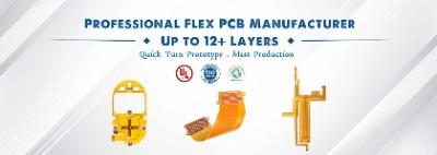
We specialize in Flex PCBs, Ridgid Flex, Long Flex PCBs and RF (radio frequency) Boards. Our engineering team has seen it all.
New Equipment | Fabrication Services
HDI PCB Manufacturer & Assembly – One-stop services from China -HDI (high-density interconnection board) is a compact circuit board designed for small capacity users. Compared with ordinary PCB, the most significant feature of HDI is that the wiri
New Equipment | Fabrication Services
XPCB Limited is one of the leading flexible PCB suppliers in China. We fabricate and assemble the most complex flexible circuit boards for harsh applications, including Oil&Gas, Medical, Security, and Aircraft & Satellite. Layer supported: 1-12 laye
Used SMT Equipment | In-Circuit Testers
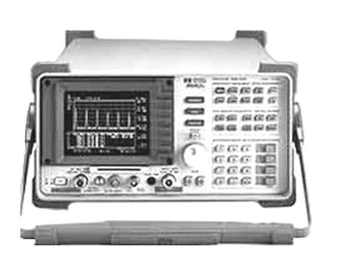
Agilent 8592L Microwave Spectrum Analyzer (9 kHz to 22/26.5 GHz) 9 kHz to 22 GHz Portable Spectrum Analyzers The Agilent 8592L is a low-cost, but full-featured, frequency accurate microwave spectrum analyzer designed to meet your general purpo
Used SMT Equipment | In-Circuit Testers
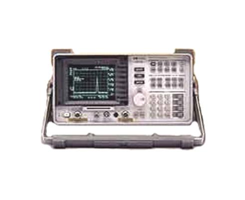
Agilent-Keysight 8590L RF Spectrum Analyzer (9 kHz to 1.8 GHz) 8590L Portable Spectrum Analyzer, 9 kHz to 1.8GHz The 8590L is a low cost, but full-featured, frequency accurate RF spectrum analyzer designed to meet your general purpose measurem
Industry News | 2009-10-17 09:43:47.0
Reduce PCB Repair Costs
Industry News | 2018-10-18 08:14:11.0
How to Prevent the Tombstone and Open Defects during the SMT Reflow Process
Technical Library | 2023-05-02 19:03:34.0
The demand for 0201 components in consumer products will increase sharply over the next few years due to the need for miniaturization. It is predicted that over 20 billion 0201 components will be used in more than one billion cell phones worldwide by the year 2003. Therefore, research and development on 0201 assembly is becoming a very hot topic. The first step to achieve a successful assembly process is to obtain a good PCB design for 0201 packages. This paper presents the data and criteria of PCB design for 0201 packages, including the pad design for 0201 components, and the minimum pad spacing or component clearance between 0201 components or between 0201 and other components. A systematic study on pad design and pad spacing was undertaken, using two test vehicles and three Design of Experiments (DOEs). In the first DOE, 2 out of 18 types of 0201 pad designs were selected based on process yield. The second DOE was focused on pad spacing, including 10mil, 8mil, 6mil and 4mil. The third experiment was final optimization, using two types of optimized pad designs with 10mil, 8mil and 6mil pad spacing. Through the above experiments, the design guideline for PCB layout for 0201 packages and the assembly process capability are identified.
Technical Library | 2020-07-15 18:29:34.0
In the early 2000s the first fine-pitch ball grid array devices became popular with designers looking to pack as much horsepower into as small a space as possible. "Smaller is better" became the rule and with that the mechanical drilling world became severely impacted by available drill bit sizes, aspect ratios, and plating methodologies. First of all, the diameter of the drill needed to be in the 0.006" or smaller range due to the reduction of pad size and spacing pitch. Secondly, the aspect ratio (depth to diameter) became limited by drill flute length, positional accuracy, rigidity of the tools (to prevent breakage), and the throwing power of acid copper plating systems. And lastly, the plating needed to close up the hole as much as possible, which led to problems with voiding, incomplete fill, and gas/solution entrapment.
HDI PCB Manufacturer & Assembly – One-stop services from China -HDI (high-density interconnection board) is a compact circuit board designed for small capacity users. Compared with ordinary PCB, the most significant feature of HDI is that the wiri

Inline 3D SPI, Standard Automatic solder paste inspection system As one of the strongest SMT 3D SPI Manufacuturer in China, we provide you all the different models of online solder paste inspection machine,we have variety of size and models of the
Training Courses | | | PCB Rework and Hand Soldering Courses
The PCB rework and hand soldering courses courses cover techniques of rework and repair of PCBs, BGAs and other electronics assemblies, and teach fundamentals of soldering of electronics assemblies.
Training Courses | | | IPC-7711/7721 Specialist (CIS)
The Certified IPC-7711/7721 Specialist (CIS) training focuses on rework of electronic assemblies and repair and modification of printed boards and electronic assemblies.
Events Calendar | Tue May 30 18:30:00 UTC 2023 - Tue May 30 18:30:00 UTC 2023 | Holtsville, New York USA
Long Island Chapter Meeting: Fine Feature Paste Printing, Stencil Design and Solder Technology
PCB Libraries, Inc. | https://www.pcblibraries.com/Forum/minimum-trace-width-spacing-for-bga_topic1556.html
Minimum Trace Width/Spacing for BGA - PCB Libraries Forum Forum Home > General > General Discussion New Posts FAQ Search Events Register Login Minimum Trace Width/Spacing for BGA
Imagineering, Inc. | https://www.pcbnet.com/capabilities/fabrication/tolerances/
″ preferred for inner layers). For scoring, minimum of .015 for outer layers and .020 for inner layers. Pad Size/Annular Ring Pad size should be at least + 0.008