Industry Directory | Manufacturer
Manufactures and Provides: thermal interface materials (TIM) including insulated-metal-substrates, gap-filling compressible phase-change pads, thermal gels-greases,(EMI/RFI) mitigation conductive gaskets and other products.
Industry Directory | Consultant / Service Provider
PWB America, Inc. is a complete solution for prototype PCB layout design, fabrication and assembly. Providing quick turn
New Equipment | Assembly Services
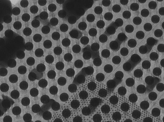
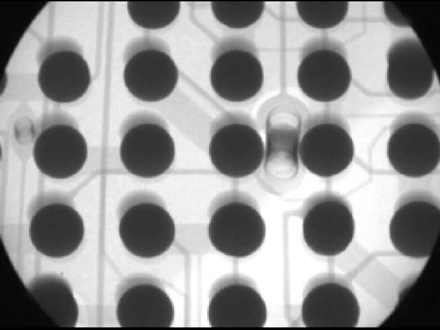
BEST can provide you with analysis services for your BGAs using x-ray equipment. We rework thousands of BGAs and POPs every year, therefore, we have the expertise in BGA X-ray inspection. BEST can be your outsourced BGA x-ray inspection source for o
New Equipment | Rework & Repair Services
Your BEST Source For High Quality Industry-Leading BGA Repair Service BEST provides industry-leading solutions for Ball Grid Array BGA Repair Services and other grid array device reworks. Our engineers have developed better processes to make our BGA
Used SMT Equipment | In-Circuit Testers
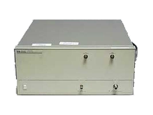
Agilent 89431A RF Section The 89431A RF Section is designed to couple with an Agilent 89410A Vector Signal Analyzer (VSA) to extend the coverage from 10 MHz to 2.65 GHz. When an Agilent 89410A VSA and an 89431A RF Section are combined, it

Used SMT Equipment | In-Circuit Testers
JDSU FireBerd 8000-CFB8000-02-C2000-V6 Communications Analyzer JDSU FB8000 The FIREBERD 8000 combines the success of two highly successful test platforms - the FIREBERD 6000A and the TestPad. As a datacom analysis module for the TestPad, the por
Industry News | 2019-12-09 14:44:26.0
The SMT Reflow Soldering Equipment (Global) award was awarded to Heller Industries by Frost & Sullivan.
Industry News | 2003-05-28 08:28:54.0
For June 2-4 (Mon. - Wed.)Design Automation Conference 2003
Technical Library | 2016-05-12 16:29:40.0
Advances in miniaturized electronic devices have led to the evolution of microvias in high density interconnect (HDI) circuit boards from single-level to stacked structures that intersect multiple HDI layers. Stacked microvias are usually filled with electroplated copper. Challenges for fabricating reliable microvias include creating strong interface between the base of the microvia and the target pad, and generating no voids in the electrodeposited copper structures. Interface delamination is the most common microvia failure due to inferior quality of electroless copper, while microvia fatigue life can be reduced by over 90% as a result of large voids, according to the authors’ finite element analysis and fatigue life prediction. This paper addresses the influence of voids on reliability of microvias, as well as the interface delamination issue.
Technical Library | 2009-04-30 18:06:24.0
This presentation surveys the most significant via and via-related laminate failure mechanisms from past to present using data from current induced thermal cycling (CITC) testing, failure analysis, and other sources. The relative life and failure modes of thru vias, buried vias, and microvias (stacked vs. non-stacked) are compared, along with the affect of structure, materials, and peak temperatures on the above. The origin of via-induced laminate failures such as "eyebrow cracks" and Pb free related internal delamination is also explored.
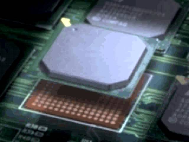
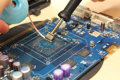
This video describes the BEST BGA rework and BGA rework services capabilities. What is described in this movie are the people, processes and tools unique to BEST and how that impacts its customers. The advanced equipment set including multiple refl
Events Calendar | Sun Apr 11 18:30:00 UTC 2021 - Sun Apr 11 18:30:00 UTC 2021 | ,
Europe Chapter Webinar: Tombstoning Components during Reflow Soldering - Causes & Cures
Events Calendar | Sun Jun 09 18:30:00 UTC 2024 - Sun Jun 09 18:30:00 UTC 2024 | Carlsbad, California USA
San Diego Chapter In-Person Event: IPC J-STD-001 Compliant Solder Pattern Calculations for DFA
Career Center | Fremont, California USA | Engineering
Job Description: • Has full ownership of HW design and release including HW specification creation, schematic generation, PCB layout, board bring up, and design verification. • Complete PCB design schematic using Orcad capture. • Complete HW desig
Career Center | Fremont, California USA | Engineering
Interprets electrical design requirements and uses Allegro design tool to create original PCB layouts, detailed fab drawings, schematics, and other design files. Work with HW design engineer to make sure PCB layout meet PCB design requirements.
ASYMTEK Products | Nordson Electronics Solutions | https://www.nordson.com/en/divisions/sonoscan/advanced-features/sonosimulator
. In the process the die stack also creates many internal interfaces where critical defects, such as voids and delaminations, can lurk
| https://www.eptac.com/wp-content/uploads/2013/08/eptac_08_21_13-1.pdf

_1.jpg)


