Industry Directory | Consultant / Service Provider
CAD Design Software products run in the AutoCAD environment.
Industry Directory | Manufacturer
D-Ying PCB manufacturers have the technological capabilities to produce your most advanced and demanding PCB products quickly
New Equipment | Test Equipment
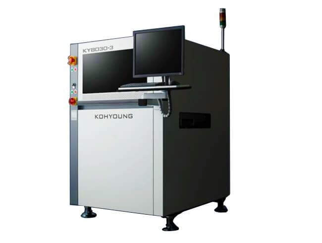
Koh Young KY8030-3 3D Inline SPI component Range: 01005 PCB size:350x330mm Dimension:1000x1335x1627mm weight:800kg Product description: Koh Young KY8030-3 3D Inline SPI, component Range: 01005, PCB size:350x330mm, Dimension:1000x1335x1627mm, weight:
New Equipment | Test Equipment
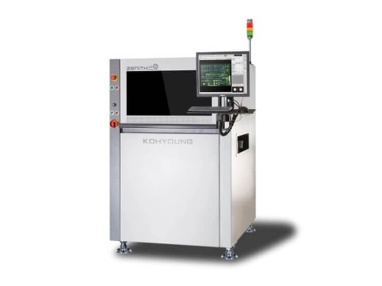
KOH YOUNG Zenith UHS 3D AOI Camera: 12M 15um Max PCB: 490 x 510 mm Weight: 600kg Dimension: 820x1265x1627 mm KOH YOUNG Zenith UHS 3D AOI KOH YOUNG Zenith UHS 3D AOI A model with 8 projections and an 8MPx camera. This model is very resistant t
Electronics Forum | Tue Jun 08 08:40:37 EDT 1999 | Wister
Hi,my master How to iron out such soldering bridge with below conditions: 1.The component(Harness)lead pitch is 2.0mm,the lead length is 3.2mm. 2.PCB width is 1.6mm.Pad size is 1.65mm.Its a single copper PCB 3.using spraying fluxer and no-clean fl
Electronics Forum | Tue Jun 08 08:38:15 EDT 1999 | Wister
Hi,my master How to iron out such soldering bridge with below conditions: 1.The component(Harness)lead pitch is 2.0mm,the lead length is 3.2mm. 2.PCB width is 1.6mm.Pad size is 1.65mm.Its a single copper PCB 3.using spraying fluxer and no-clean fl
Used SMT Equipment | Soldering - Selective
ACE KISS 104 Selective Solder Model: KISS 104 Vintage: 2007 Voltage: 115/120 Two (2) pots - One leaded, one lead-free FEATURES: The KISS-104 is a fully configured In-Line SMEMA compatible Selective Soldering Machine ready to produce your produ
Industry News | 2018-10-18 08:34:52.0
How to Prevent Solder Bridging in 3528 PLCC6 RGB LEDs?

Parts & Supplies | Chipshooters / Chip Mounters
> JUKI ESL13000000 VACUUM PAD 15 JUKI ESL13000100 PHOTO MICRO SENSOR A JUKI ESL13001000 TUBE union (KL700) JUKI ESL130011A0 CONVEYOR MOTOR (KZ500) JUKI ESL13002000 CLAMP LEVER JUKI ESL13003000 T TYPE NUT JUKI ESL130031A0 OPERATION PANEL (KL700) JUKI

Parts & Supplies | Pick and Place/Feeders
SM8mm Feeder Cylinder J90650160c J9065335A SMC Cj2r10-8.3D-Krj Original New or Copy New are in stock, please contact me : alice@smtpartssupply.com Description: SAMSUNG SM Feeder cylinder Part No: J90650160C J9065335A Condition: original new / co
Technical Library | 1999-05-07 08:45:39.0
Fine pitch SMT devices, although certainly not new, present more of an assembly processing challenge than 50 mil pitch devices. In fact it seems that the finer the pitch the more difficult or narrower the process window becomes. Besides the pitch of the leads being less on fine pitch devices narrower pad width on the board is typical. With fine pitch designs the board fabrication process is also stressed in that the strip of mask between the pads is designed narrower, the alignment of the mask to copper becomes more critical
Technical Library | 2020-08-27 01:22:45.0
Initially adopted internal specifications for acceptance of printed circuit boards (PCBs) used for wire bonding was that there were no nodules or scratches allowed on the wirebond pads when inspected under 20X magnification. The nodules and scratches were not defined by measurable dimensions and were considered to be unacceptable if there was any sign of a visual blemish on wire-bondable features. Analysis of the yield at a PCB manufacturer monitored monthly for over two years indicated that the target yield could not be achieved, and the main reasons for yield loss were due to nodules and scratches on the wirebonding pads. The PCB manufacturer attempted to eliminate nodules and scratches. First, a light-scrubbing step was added after electroless copper plating to remove any co-deposited fine particles that acted as a seed for nodules at the time of copper plating. Then, the electrolytic copper plating tank was emptied, fully cleaned, and filtered to eliminate the possibility of co-deposited particles in the electroplating process. Both actions greatly reduced the density of the nodules but did not fully eliminate them. Even though there was only one nodule on any wire-bonding pad, the board was still considered a reject. To reduce scratches on wirebonding pads, the PCB manufacturer utilized foam trays after routing the boards so that they did not make direct contact with other boards. This action significantly reduced the scratches on wire-bonding pads, even though some isolated scratches still appeared from time to time, which caused the boards to be rejected. Even with these significant improvements, the target yield remained unachievable. Another approach was then taken to consider if wire bonding could be successfully performed over nodules and scratches and if there was a dimensional threshold where wire bonding could be successful. A gold ball bonding process called either stand-off-stitch bonding (SSB) or ball-stitch-on-ball bonding (BSOB) was used to determine the effects of nodules and scratches on wire bonds. The dimension of nodules, including height, and the size of scratches, including width, were measured before wire bonding. Wire bonding was then performed directly on various sizes of nodules and scratches on the bonding pad, and the evaluation of wire bonds was conducted using wire pull tests before and after reliability testing. Based on the results of the wire-bonding evaluation, the internal specification for nodules and scratches for wirebondable PCBs was modified to allow nodules and scratches with a certain height and a width limitation compared to initially adopted internal specifications of no nodules and no scratches. Such an approach resulted in improved yield at the PCB manufacturer.

About more detail for the PCB destacker check the link? https://www.ascen.ltd/Products/Automatic_SMT_equipment/PCB_loader/125.html PCB destacker/PCB bare board unloader unloading bare board to replace the PCB magazine unloader machine for the PCB bar

1200MM/1500MM Online SPI , Big Size Solder Paste Inspection Machine mail: sales@smtlinemachine.com whatapp/wechat:+8613537875415 Specification: 技术参数/Parameters 技术平台/Technology Platform super big size platform 适用
regulations. Long before the debate over lead-free all
QYSMT SOLUTION USA LLC / Qinyi Electronics Co.,Ltd | https://www.qy-smt.com/shop/l166e021000-width-link-belt-147372?page=75&category=1168
JUKI Width Link Belt L166E021000 | QYSMT × Home About US ABOUT US FAQ SMT spare parts SMT Surplus equipments SMT peripheral equipments News Contact US 0 0 Sign in Contact Us Products Others SMT parts Width Link Belt Public Pricelist Public
ASYMTEK Products | Nordson Electronics Solutions | https://www.nordson.com/en/divisions/asymtek/products/conformal-coating-systems/laser-fan-width-options
Width Options Laser Fan Width Options improve repeatability for conformal coating applications and lead to higher yield and increased traceability The unmatched performance of Nordson ASYMTEK's


winsouce.jpg)