Industry Directory | Other / Consultant / Service Provider / Media / Publisher / Online Resource
PCB Libraries' "Footprint Expert" suite uses CAD LEAP(tm) Technology to greatly simplify footprint and 3D STEP model creation; it is used by tens of thousands of PCB designers and engineers all over the world.
Industry Directory | Manufacturer
One-Stop PCB Manufacturer, PCB Assembly and PCB Prototype Service in USA. Our Expertise Are in Electronics Manufacturing Services. Call Now.
New Equipment | Rework & Repair Equipment
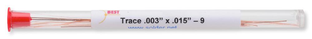
BEST PCB circuit traces are designed to help you repair, replace and modify circuit traces on PCBs. These materials allow you to meet original PCB quality standards as the board side is microetched for improved bonding area and bond strength. The re
New Equipment | Rework & Repair Equipment
The BEST PCB circuit trace repair kit gives you the tools you need for fast modification and repair of PCB circuit traces. Our online PCB repair training videos, our master instructors along with these materials allows you to meet the original PCB qu
Used SMT Equipment | X-Ray Inspection
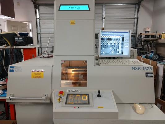
This is a used NXR-1525 Xray System can be used to for PCB X-ray inspection of BGA and other SMD Devices. It is a high resolution X-ray system that can show inner layer traces of the Circuit Board. The date of manufacture is September 1999. It
Industry News | 2018-02-12 12:28:00.0
GPD Global introduces its NEW full-featured benchtop dispensing robot system: Catalina. A benchtop system does not mean "no features". This compact and efficient semi-auto dispense robot provides you with numerous standard features: automatic vision, laser surface sensing, and automatic nozzle alignment and calibration.
Industry News | 2018-09-06 12:12:07.0
GPD Global offers the ideal tabletop robots (Catalina Series) for precision dispensing.
Technical Library | 2011-11-25 16:07:47.0
The article presents virtual and real investigations related to current capacity and fusing of PCB traces in high power applications and is based on a scientific paper delivered by authors at SIITME 2010 in Romania. The reason of performing the research a
Technical Library | 2021-10-12 18:01:49.0
The existence of counterfeit products, e.g., integrated circuits (ICs) and printed circuit boards (PCBs), in the modern semiconductor supply chain has seriously jeopardized the security and reliability of electronic systems, and has also caused the loss of suppliers' profit and reputation. Most of existing research papers prevent or detect counterfeit IC and PCB substrate separately, without testing the PCB as a whole, and often require the assistance of external equipment. In this article, a novel ring oscillator- based PCB authentication (ROPA) methodology to detect counterfeit PCB through supply chain is proposed, which ...

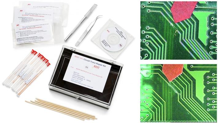
PCB pad circuit repair using epoxy. Using multiple angles including overhead and from both right and left angles the BEST instructor staff demonstrates plainly how to repair a PCB pad using the epoxy method. This method is per IPC 7721 4.4.1. http://
PCB pad circuit repair using epoxy. Using multiple angles including overhead and from both right and left angles the BEST instructor staff demonstrates plainly how to repair a PCB pad using the epoxy method. This method is per IPC 7721 4.4.1. http://
Training Courses | | | PCB Rework and Hand Soldering Courses
The PCB rework and hand soldering courses courses cover techniques of rework and repair of PCBs, BGAs and other electronics assemblies, and teach fundamentals of soldering of electronics assemblies.
Training Courses | | | PCB Rework and Hand Soldering Courses
The PCB rework and hand soldering courses courses cover techniques of rework and repair of PCBs, BGAs and other electronics assemblies, and teach fundamentals of soldering of electronics assemblies.
Career Center | Fremont, California USA | Engineering
Interprets electrical design requirements and uses Allegro design tool to create original PCB layouts, detailed fab drawings, schematics, and other design files. Work with HW design engineer to make sure PCB layout meet PCB design requirements.
Career Center | Auckland, New Zealand | Engineering
NAVMAN PCBA NPI Engineer Reporting To: PCBA NPI Technical Leader Primary Objective: Transition of PCBs from R&D design to a manufacturable state conforming to all facets of PCBA production Secondary: Develop DFM & best practice guidelines Res
Career Center | Damascus, Syria | Engineering,Maintenance,Production,Technical Support
Experience : 1- PCB Test Engineer For Telecom Products And TV - LCD Manufacturing as follow : - In-Circuit and Automatic Test Equipment Test - in-circtuit Emulator - Function Test - Automatic Optical Inspection Test - Toubleshooting Axial
Career Center | Newport Beach, California USA | Engineering,Management,Production
KEVIN RAGER P.O.BOX 7878, NEWPORT BEACH, 949 922 8997, KEVIN.RAGER@EDA-INC.US OBJECTIVE I am trying to find a consistent work flow that provides mentally challenging yet stimulating experiences in design and prototype development. EXPERIENCE 1997
New Methods of Testing PCB Traces Capacity and Fusing New Methods of Testing PCB Traces Capacity and Fusing by: Norocel Codreanu, Radu Bunea, Paul Svasta; "Politehnica" University of Bucharest, Center for Technological Electronics
Imagineering, Inc. | https://www.pcbnet.com/capabilities/fabrication/tolerances/
PCB Fabrication Tolerances | Imagineering Skip to main content Resources Support Contact Us FAQs Live Chat My Account 847-806-0003 Menu PCB Capabilities Fabrication Technology Roadmap Materials Available HDI Tolerances
| https://www.smtfactory.com/PCB-Protector-pl3958223.html
. Normally, the film is applied at thickness of 25-250µm protecting and covering solder joints, the leads of electronic components, exposed traces and PADs, and other metallised areas from corrosion, so as to extend the working life of the PCB , and
.jpg)