Microwave Plasma System for assembly cleaning prior to wirebond, attach, encapsulation, and underfill.
Industry Directory | Manufacturer
Plasmatreat is the global market leader in developing surface treatment solutions with atmospheric and low pressure plasma technology
New Equipment | Cleaning Equipment
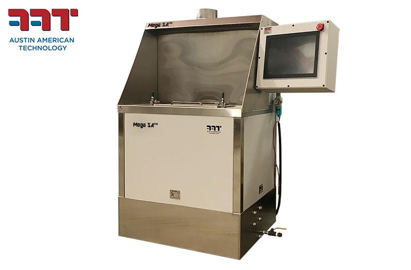
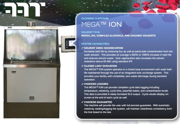
Austin American Technology’s Mega SA® cleaning system is designed for primary defluxing and final cleaning prior to sealing. It uses semi-aqueous chemistries requiring a water rinse. The Mega SA® is compatible with Terpenes, and petroleum-based solve
New Equipment | Cleaning Equipment
World’s First Cleaner & ROSE Tester Removes Fluxes Performs IPC ROSE Test Closed Loop Operation - No Drains Aqueous or Organic Solvents Stainless Steel Construction Automatic Wash/Rinse/Test/Dry 230VAC, 10AMP, 50/60Hz
Industry News | 2018-10-18 19:57:48.0
Industry-leading associations IPC and SMTA jointly announce the High-Reliability Cleaning and Conformal Coating Conference, scheduled to take place November 13-15, 2018 at Chicago Marriott, Schaumburg, Illinois. The conference is focused on the cleanliness of highly dense electronic assemblies to achieve quality and reliability within the stated in-field environment.
Industry News | 2025-02-17 18:07:05.0
See this unique nozzle cleaning system and speak with our experts at IPC APEX booth 3200
Technical Library | 2020-08-27 01:22:45.0
Initially adopted internal specifications for acceptance of printed circuit boards (PCBs) used for wire bonding was that there were no nodules or scratches allowed on the wirebond pads when inspected under 20X magnification. The nodules and scratches were not defined by measurable dimensions and were considered to be unacceptable if there was any sign of a visual blemish on wire-bondable features. Analysis of the yield at a PCB manufacturer monitored monthly for over two years indicated that the target yield could not be achieved, and the main reasons for yield loss were due to nodules and scratches on the wirebonding pads. The PCB manufacturer attempted to eliminate nodules and scratches. First, a light-scrubbing step was added after electroless copper plating to remove any co-deposited fine particles that acted as a seed for nodules at the time of copper plating. Then, the electrolytic copper plating tank was emptied, fully cleaned, and filtered to eliminate the possibility of co-deposited particles in the electroplating process. Both actions greatly reduced the density of the nodules but did not fully eliminate them. Even though there was only one nodule on any wire-bonding pad, the board was still considered a reject. To reduce scratches on wirebonding pads, the PCB manufacturer utilized foam trays after routing the boards so that they did not make direct contact with other boards. This action significantly reduced the scratches on wire-bonding pads, even though some isolated scratches still appeared from time to time, which caused the boards to be rejected. Even with these significant improvements, the target yield remained unachievable. Another approach was then taken to consider if wire bonding could be successfully performed over nodules and scratches and if there was a dimensional threshold where wire bonding could be successful. A gold ball bonding process called either stand-off-stitch bonding (SSB) or ball-stitch-on-ball bonding (BSOB) was used to determine the effects of nodules and scratches on wire bonds. The dimension of nodules, including height, and the size of scratches, including width, were measured before wire bonding. Wire bonding was then performed directly on various sizes of nodules and scratches on the bonding pad, and the evaluation of wire bonds was conducted using wire pull tests before and after reliability testing. Based on the results of the wire-bonding evaluation, the internal specification for nodules and scratches for wirebondable PCBs was modified to allow nodules and scratches with a certain height and a width limitation compared to initially adopted internal specifications of no nodules and no scratches. Such an approach resulted in improved yield at the PCB manufacturer.

Designed for wafer processing, Nordson MARCH's SPHERE™ series plasma systems, the StratoSPHERE offers superior plasma treatment for high-throughput advanced semiconductor packaging applications. The StratoSPHERE plasma system is ideal for wafer pro
40731 | https://www.smta.org/harsh/Harsh-Environments-Program-2019.pdf?v=20052905555
Surface Mount Technology Association (SMTA)
| http://www.thebranfordgroup.com/dnn3/Auction/TSLE0523.aspx
. Sn - Osp manual electroplating w/post-cleaning + dryer Laif Cu & Tn Pattern Plate Electroplating Line PVA Tepla Plasma-Etch System Hot Air Levelling Laif HASL Pre-Clean Line Cemco Quicksilver Hot Air Leveller lead free Pola e Massa HASL post-cleaning Artwork


