Industry Directory | Manufacturer
PCB solder mask, PCB etching resist ink, LED white solder mask. UV curing solder mask, UV curing anti-acid etching resist ink
Industry Directory | Manufacturer
The exclusive supplier of SIPAD Solid Solder Deposit in North America and the only SIPAD Solid Solder Deposit (SSD) coating service bureau in the world.
New Equipment | Education/Training
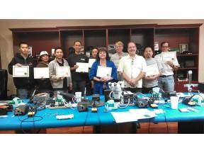
In this One-Day class you will learn successful techniques to re-ball BGA Components. Both Lead and Lead Free Solder Balls will be covered. The student will have an opportunity to use and evaluate some of the most popular BGA rework fixtures on the
New Equipment | Education/Training
This course is designed for students that require the hands-on skill and knowledge to reliably remove and install many types of the most complex BGA components. Students are taught methods for safe and reliable BGA component rework using a top of the
Electronics Forum | Mon Aug 09 18:03:28 EDT 1999 | Earl Moon
| | I am having cleaning problems when processing PCB's which have | | TAIYO solder mask on them. After processing, hand soldering and | | cleaning, a sticky residue is remains, resulting in a cosmetically poor finish with tide marks etc. Other solde
Electronics Forum | Tue Aug 10 16:01:12 EDT 1999 | Earl Moon
| | | | | | I am having cleaning problems when processing PCB's which have | | | | | | TAIYO solder mask on them. After processing, hand soldering and | | | | | | cleaning, a sticky residue is remains, resulting in a cosmetically poor finish with tid
Industry News | 2018-10-18 08:04:17.0
Influences of the solder material for the wave soldering machine soldering quality
Industry News | 2018-12-08 03:29:29.0
SMT Dictionary – Surface Mount Technology Acronym and Abbreviation

Parts & Supplies | Pick and Place/Feeders
The definition of SMT SMT is the surface assembly technology,surface mount technology(surface mount technology)(Surface Mounted Technology abbreviation),is currently the most popular electronic assembly industry,a technology and technology. What a
Technical Library | 2007-02-01 10:08:40.0
The increased replacement of high lead count SMT devices with BGAs and other high ball count area array packages has brought increased challenges to PCB rework and repair. Often solder mask areas surrounding BGA pad areas are damaged when components are removed.
Technical Library | 2016-11-30 21:30:50.0
Mid-chip solder balling is a defect typically associated with solder paste exhibiting poor hot slump and/or insufficient wetting during the reflow soldering process, resulting in paste flowing under the component or onto the solder resist. Once molten, this solder is compressed and forced to the side of the component, causing mid-chip solder balling.This paper documents the experimental work performed to further understand the impact on mid-chip solder balling from both the manufacturing process and the flux chemistry.
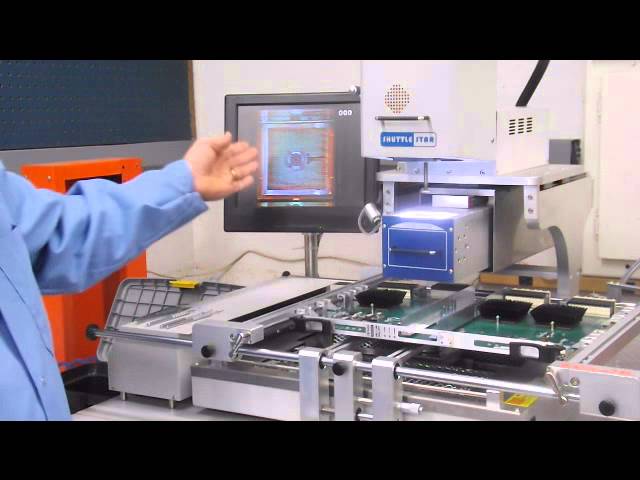
Dennis Odonnell , Vice President of Precision PCB Services, Inc., Oroville CA Explains How to Evaluate a BGA Rework Station ! #BGA Rework Stations http://www.pcb-repair.com/bga-rework-station/
Dennis Odonnell , Vice President of Precision PCB Services, Inc., Oroville CA Explains How to Evaluate a BGA Rework Station ! #BGA Rework Stations http://www.pcb-repair.com/bga-rework-station/
Training Courses | | | PCB Rework and Hand Soldering Courses
The PCB rework and hand soldering courses courses cover techniques of rework and repair of PCBs, BGAs and other electronics assemblies, and teach fundamentals of soldering of electronics assemblies.
Training Courses | | | PCB Rework and Hand Soldering Courses
The PCB rework and hand soldering courses courses cover techniques of rework and repair of PCBs, BGAs and other electronics assemblies, and teach fundamentals of soldering of electronics assemblies.
Events Calendar | Mon Apr 12 00:00:00 EDT 2021 - Mon Apr 12 00:00:00 EDT 2021 | ,
Europe Chapter Webinar: Tombstoning Components during Reflow Soldering - Causes & Cures
Events Calendar | Tue Apr 13 00:00:00 EDT 2021 - Tue Apr 13 00:00:00 EDT 2021 | ,
Boston Chapter Webinar: Cleaning Chemistry For PWB and Rework - Part 2, session 1
Career Center | Space Coast, Florida USA | Engineering,Research and Development
Board Level Assembly BGA Expert! We are in need of an Electronic Packaging or Advanced Manufacturing Engineer to work with the Advanced Manufacturing Technology Group of a major Florida based Communications company. Support IR&D and Program activit
Career Center | Melbourne, Florida USA | Engineering
Advanced Manufacturing Technology Position Description Job Description: AMT Engineer � Level 4 Support IR&D and Program activities Division wide working on the development, qualification, and implementation of electronic packaging technologies, wi
Career Center | , Israel | Engineering,Maintenance,Technical Support
I was born on June , 1972 in Khmelnitsky city , Ukraine . I am male. From 1979 to 1987 I was studying at secondary school #7, having finished which I entered the Technical College of Khmelnitsky in specialty Machine Tools with Computer Numeric Contr
Thermal Spot Curing of Adhesives with Photonic Energy; a novel fiber delivery method of radiant heating to accelerate the polymerization of thermally active adhesives Thermal Spot Curing of Adhesives with Photonic Energy; A novel fiber delivery
Heller Industries Inc. | https://hellerindustries.com/solder-balls-defects/
Solder Ball Defects - Heller Home » Solder Ball Defects Re-printed in partnership with ITM Solder Ball Defects Defect: solder balls Solder balls are very small fines of solder that have separated from the main body that forms the joint
PCB Libraries, Inc. | https://www.pcblibraries.com/forum/RSS_blind-via-with-smaller-solder-mask-opening_topic1110.xml
. I did the same thing once and the bare boards got to assembly and rejected. Tried to go back to the fabrication shop but they turned me down saying that the solder mask has been cured and there was nothing they could do.


