
Industry Directory | Consultant / Service Provider
PCB Electronics Manufacturing Automation Software for EMS, OEM & ODM manufacturers. Over 3000 customers worldwide!
Industry Directory | Equipment Dealer / Broker / Auctions
FabExchange uses our extensive global connections to source the best tools and buyers for semiconductor manufacturing equipment. Our unique combination of brokerage and auction services equips us to execute on any project.
New Equipment | Fabrication Services
High frequency RF, Microwave Printed Circuit Board Design, FAB PNC can provide you with your High Frequency RF PCB and Microwave PCB needs. Our advanced Technologies have made us a leader in the RF/Microwave PCB industry processing FR4 and Rogers Ma
Electronics Forum | Wed Dec 20 15:21:06 EST 2000 | OS
How should OSP PCB be handled, when stored; and during manufactruing process on production floor?
Electronics Forum | Tue Sep 26 20:19:51 EDT 2000 | Dave F
Never heard of N-Tech. Whose material do they use? Two common materials are: Imidazole (Via Systems) and Entek (Enthone) OSP is a lacquer that fabs apply to boards by either spraying or dipping. What thickness control does your fab use? For inst
Used SMT Equipment | Chipshooters / Chip Mounters
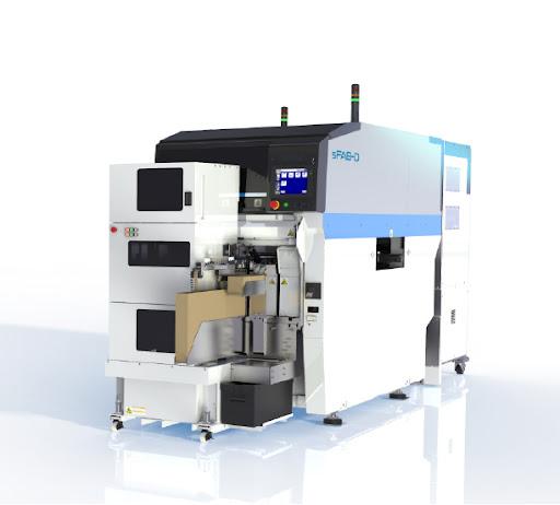
sFAB-D machines have continued to evolve since their release to the market. They are able to insert parts into various panels with a wide range of support in part packaging. As an entry model, sFAB-SH machines are now added into the same product line
Used SMT Equipment | Pick and Place/Feeders
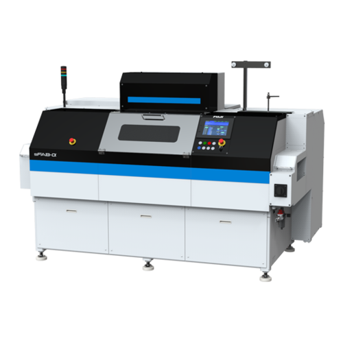
FUJI sFAB-a (alpha) odd-form inserter Surface mount technology continues to grow as the most popular method for assembling electronic parts, and the quantity of discrete parts used has reduced year by year. However, discrete parts do continue to
Industry News | 2002-03-29 08:28:28.0
Has Found a Buyer for its Wafer Fabrication Facility in Plymouth, England
Industry News | 2003-02-10 08:20:11.0
Leading Suppliers of Chemistries for Circuit Board Processing Have Entered a Selling and Services Deal
Technical Library | 1999-08-09 11:09:42.0
Organic Solderability Preservatives (OSPs), also known as anti-tarnish, on bare copper printed circuit boards (PCBs) are becoming more prevalent in the electronics industry as the low-cost replacement to Hot Air Solder Leveling (HASL). Introducing the anti-tarnish alternative into the customer sites requires working closely with the coating supplier, assembler, and Original Equipment Manufacturer (OEM) to gain a mutual understanding of respective processing concerns and finished product requirements.
Technical Library | 2017-11-01 17:06:38.0
Over fifteen years has passed since North America and Europe ceased being the center of worldwide PCB fabrication, and were supplanted by a Far East market with low cost labor, more relaxed environmental requirements, and strong government support. In just a few short years, the superior cost advantages of this new dynamic put volume PCB production in the West out of business, aside for the military and specialty technology applications contained in the few shops that continue to exist today.Recently, however, the conditions which created the current equilibrium appear to be shifting again. In this new dynamic, automation, innovative green wastewater technologies, and next generation process equipment innovations have combined to make new factories capable of achieving rapid ROI for PCB fabrication almost anywhere. This paper means to illustrate this new dynamic, and provide case study examples from the new greenfield installation at the company captive facility in New Hampshire.

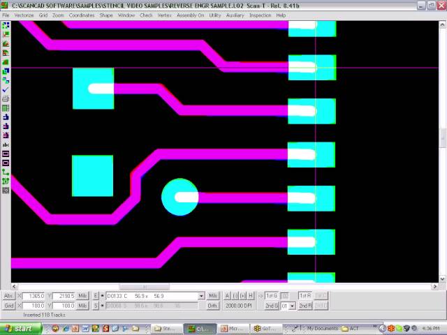
ScanCAD offers a family of modular products to assist in the PCB Reverse Engineering Process. Start from a PCB or set of films to generate all the needed data and files (from BOM to Schematic) to manufacture or repair legacy parts. Precise form, fi
Events Calendar | Tue Jul 18 00:00:00 EDT 2023 - Tue Jul 18 00:00:00 EDT 2023 | Chippewa Falls, Wisconsin USA
UMW Chapter In-Person Event: PCB 101 Workshop and Tour at TTM Chippewa Falls
Events Calendar | Tue Apr 13 00:00:00 EDT 2021 - Tue Apr 13 00:00:00 EDT 2021 | ,
Boston Chapter Webinar: Cleaning Chemistry For PWB and Rework - Part 2, session 1
Career Center | Rochester, New York USA | Engineering
Kodak ISS continues to experience significant growth. As part of Kodak's digital growth strategy, ISS develops, manufactures and markets imaging sensor devices that are a critical component in a broad range of imaging products including digital camer
Career Center | Switzerland, Switzerland Switzerland | Engineering,Production
Sr. Process Engineer Key position producing IGBT�s and Diodes, 1,2kV to 6kV, 5�. Current wafer production 70,000-100,000, expansion to 280,000 wafers/year. BiMOS fab. Salary: 75-100,000Sfr/year + 10-15% bonus. 1 month vacation. Daytime 8-17.00 wi
Career Center | Saginaw, Texas USA | Engineering,Maintenance,Management,Production,Quality Control,Technical Support
Over 20 Years Experience with SMT Processes at Large and Medium Sized Companies like Hitachi, Nokia, Siemens, and Variosystems Troubleshooting SMT Process Deficiencies and Recommending Short Term and Long Term Solutions. Developing Technical
Career Center | Rochester, New York USA | Engineering
I have done my undergraduate studies in Mechanical Engineering. I am pursuing my Master's Program in Electronics Packaging. I am currently working as a Research Assistant for RIT-CEMA (Center for Electronics Manufacturing and Assembly). My research
ATTENDANT WET CHEMICAL PROCESSES) Hole wall preparatio
Heller 公司 | http://hellerindustries.com.cn/Vacuum-Void-Reduction-Reflow.pdf
The Effect of Vacuum Reflow Processing On Solder Joint Voiding And Thermal Fatigue Reliability To be published in the Proceedings of SMTA International, September 17 - 21, 2016, Rosemont, IL
Imagineering, Inc. | https://www.pcbnet.com/blog/understanding-the-pcb-fabrication-process-from-design-to-delivery/
manufacturers are typically located outside the U.S . This post provides an overview of the PCB fabrication process, including pre-processing steps


winsouce.jpg)