Industry Directory | Consultant / Service Provider
Manufacturer of non-contact 3D measurement systems based on low coherence interferometry technology. Products include optical profilometers, OCT systems, and metrology software.
Industry Directory | Consultant / Service Provider / Manufacturer
From the Irvine, CA office Nanovea began designing and manufacturing instruments after years of experience in providing solutions for profilometry, mechanical and tribology applications.
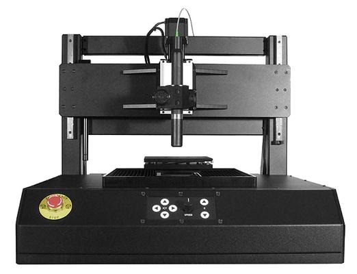
Nanovea 3D Non-Contact Profilometers are designed with leading edge optical pens using superior white light axial chromatism. Nano through macro range is obtained during measurement (Profile Dimension, Roughness Finish Texture, Shape Form Topography,

Cyber Technologies in-line solutions provide non-contact measurement capability for quickly scanning any surface. The system produces a high-resolution, two-dimensional profile or 3D raster scan. It combines digital laser sensor technology, a compute
Electronics Forum | Fri Oct 23 16:01:18 EDT 1998 | Earl Moon
| I need some info on how to stop the bridges I'm having on | radial and axial parts that are in the same place on every board. I'm also having problems with sot-25 bridging. I'm using a Electrovert E-pak. I tried leveling the machine,solder pot, an
Electronics Forum | Fri Jun 25 12:01:49 EDT 1999 | Earl Moon
| | Dear John/Earl | | | | Thanks for your clarifications. To me also the problem does not seem to be linked with the PCB. The Pre heater temp. is set at | | 450 degree C. We are using Alpha Aq. cleanable flux. Can you elaborate on the Desired
Used SMT Equipment | AOI / Automated Optical Inspection
Really high quality used solder paste inspection with 1 year warranty Features BF-SPIDER - SOLDER PASTE INSPECTION DESCRIPTION: 1. The newly developed Phase Measurement Profilometer Technology ensures high inspection repeatability. 2. Advan
Industry News | 2011-06-14 14:37:55.0
The white light axial chromatism technique utilized by Nanovea’s 3D Non Contact Profilometers has become widely known as a vital bench top research and verification tool. It is now the Automated Optical Inspection (AOI) environments that have begun to acknowledge Nanovea’s superior capability. Unlike the traditional vision and laser systems that typically sacrifice one feature for another, speed or resolution, Nanovea provides both. Vision and laser systems also have very limited automated surface measurement options, where as Nanovea’s system provides a wide range including: Profile, Dimension, Roughness, Shape & Form, Flatness & Planarity, Volume Area, Step-Height Depth and Thickness. And keep in mind, the technique utilized by Nanovea’s inspection system has the superior ability to measure nearly any material surface and zero influence from sample reflectivity or absorption.
Industry News | 2012-01-20 11:37:53.0
Nanovea today announced the arrival of the N3 line dedicated to providing high-end measurement technology to the broader market. Nanovea has fully automated their measurement techniques while designing to price in the $20K market.
Technical Library | 2018-05-17 11:14:52.0
Intermetallic compound (IMC) growth is being studied in earnest in this past decade because of its significant effect the solder joint reliability. It appears that from numerous investigations conducted, excessive growth of IMC could lead to solder joint failure. Leading to this, many attempts has been made to determine the actual IMC thickness. However, precise and true representation of the growth in the actual 3D phenomenon from 2D cross-section investigations has remained unclear. This paper will focus on the measuring the IMC thickness using 3D surface profilometer (Alicona Focus G4). Lead free solder, Sn3.0Ag0.5Cu (SAC305) was soldered onto copper printed circuit board (Cu PCB). The samples were then subjected to thermal cycle (TC) storage process with temperature range from 0 °C to 100 °C for 200 cycles and up to 1000 cycles were completed.
Technical Library | 2021-11-03 17:05:39.0
Additively printed circuits provide advantages in reduced waste, rapid prototyping, and versatile flexible substrate choices relative to conventional circuit printing. Copper (Cu) based inks along with intense pulsed light (IPL) sintering can be used in additive circuit printing. However, IPL sintered Cu typically suffer from poor solderability due to high roughness and porosity. To address this, hybrid Cu ink which consists of Cu precursor/nanoparticle was formulated to seed Cu species and fill voids in the sintered structure. Nickel (Ni) electroplating was utilized to further improve surface solderability. Simulations were performed at various electroplating conditions and Cu cathode surface roughness using the multi-physics finite element method. By utilizing a mask during IPL sintering, conductivity was induced in exposed regions; this was utilized to achieve selective Ni-electroplating. Surface morphology and cross section analysis of the electrodes were observed through scanning electron microscopy and a 3D optical profilometer. Energy dispersive X-ray spectroscopy analysis was conducted to investigate changes in surface compositions. ASTM D3359 adhesion testing was performed to examine the adhesion between the electrode and substrate. Solder-electrode shear tests were investigated with a tensile tester to observe the shear strength between solder and electrodes. By utilizing Cu precursors and novel multifaceted approach of IPL sintering, a robust and solderable Ni electroplated conductive Cu printed electrode was achieved.
ASYMTEK Products | Nordson Electronics Solutions | https://www.nordson.com/en/divisions/sonoscan/about/patent-list
. This list will be occasionally be updated as pending patents are issued. U.S. PATENT NO. 8,794,072 B2 Scanning Acoustic Microscope with Profilometer Function U.S. PATENT NO


winsouce.jpg)


