Industry Directory | Consultant / Service Provider / Manufacturer
PCB & Cable Assemblers TMS was established over 25 years ago in Wokingham , Berkshire, as a cable assembly company trading under the name Robinson's Computer Technical Services. In 1993 the trading name was changed to Robinson's D
Ruggedised electronic and fibre optic connectors and cable assemblies for demanding applications in medical, test & measurement, broadcast and industrial markets.

The PCB Footprint Expert is a powerful CAD library development tool powered by our own proprietary CAD LEAP Technology (Libraries Enhanced with Automated Preferences). It is packed with very powerful advanced library management features that cuts foo

New Equipment | Education/Training
Now updated to Revision F of the latest IPC-A-610F and J-STD-001F – the IPC Training & Reference Guide illustrates critical acceptance criteria for the evaluation of through-hole solder connections. With 30 pages and a compact size at 5.5 x 8.5 inch
Electronics Forum | Thu Feb 05 05:27:55 EST 2004 | dszeto
We have recent customer asking for PCB's PTH hole size related to soldered wire AWG 18-26. Please kindly advise any international standard for captioned issue. Thanks!
Electronics Forum | Thu Feb 05 08:39:16 EST 2004 | davef
IPC-2222 - Sectional Design Standard For Printed Board For Organic Printed Boards, Table 9-3 � Plated Through Hole Diameter To Lead Diameter Relationships will give you the standard information you require.
Used SMT Equipment | AOI / Automated Optical Inspection
Omron VT-RNS-PTH-P Desktop AOI on sale. 1.Vintage: 2009 2.Condtion: Brand-new 3.Max.PCB Size: 650x550mm 4.Q'ty: 2 units For more details, please contact us.
Used SMT Equipment | AOI / Automated Optical Inspection
We are selling 1 set of Omron VT-RNS-PTH-L desktop AOI. 1.Vintage: July, 2009 2.Condition: BRAND NEW 3.Max. PCB Size: 650 x 550mm 4.Steel table included For more details, please contact us.
Industry News | 2008-05-01 11:14:36.0
Component packaging technology continues to decrease in size (length, width, thickness), interconnection density per unit area is increasing (thinner PCB�s, smaller lines & spaces), functional performance is increasing (thermal, mechanical, electrical) at the same time as assembly processes are changing to lead-free assembly and other legislated requirements.
Industry News | 2010-09-30 00:35:51.0
The new E revisions of IPC’s popular desk reference manuals, IPC-DRM-PTH, Through-Hole Solder Joint Evaluation Training & Reference Guide and IPC-DRM-SMT, Surface Mount Solder Joint Evaluation Training & Reference Guide have been released.
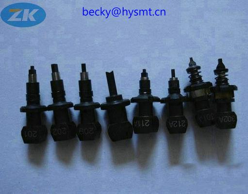
Parts & Supplies | Pick and Place/Feeders
Which series nozzles could be used for Phlips Topaz and Emerald machine As we know, many parts are compatible for Yamaha and Philips machines, but some models their nozzles are not generic.So which series nozzles could be used for Phlips Topaz and
Technical Library | 2021-07-13 19:59:34.0
We have investigated the processing of lead-zirconate-titanate-based thick films by inkjet printing Pb (Zr0.53Ti0.47)0.98Nb0.02O3 with a 6 mol% excess of PbO nanosized powder dispersed in water. Differentwaveforms were employed to determine the optimum size and shape of the drops. A uniform, defect-free pattern with dimensions of 4 mm × 4 mm can be printed using 20 V and a drop spacing of 20 μm. The inkjet-printed films were heated to 400 °C to remove the organics and subsequently sintered at 750 and 850 °C. The correlations between the density, grain size and electromechanical properties of the thick films and bulk ceramics are qualitatively discussed. A thickness coupling factor of 46% was obtained for a 15-μm-thick film sintered at low temperature of 850 °C, which is comparable to the value of the bulk ceramic with an identical nominal chemical composition. Our results are important for the economic and environmental-benign printing of piezoelectric materials applicable in variety of electronic devices, such as sensors, actuators, transformers, piezoelectric energy harvesters and transducers.

The PCB Footprint Expert is a powerful CAD library development tool powered by our own proprietary CAD LEAP Technology (Libraries Enhanced with Automated Preferences). It is packed with very powerful advanced library management features that cuts foo
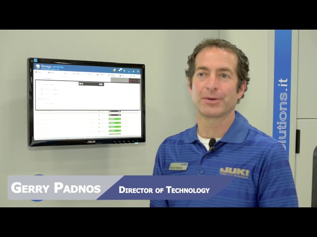
JUKI Automation Systems at the IPC Apex 2015; showcasing Intelligent Storage Systems.
Career Center | St. Charles, Illinois USA | Engineering,Maintenance,Production
An established Contract Electronics Mfg. in the Western Suburbs of Chicago is looking for an individual that values hard work and understands the opportunity of working with a mid-sized company for growth potential. Long-term full-time position 8:00a
Career Center | , | Engineering,Production
Project Management, SMT Process Engineering
Career Center | Shen Zhen, China | Management,Sales/Marketing
Working in GLORYPCB for 10 years.knowing electronic supply chain very well. especially for PCB PCBA assembly and other Electronic Manufacturing Service.Glorypcb is a professional electronic manufacturer located in Shenzhen with three facilities.offe
| https://www.eptac.com/faqs/soldertips/soldertip/soldertip-36-wave-soldering-insufficient-fill-and-voids-in-pth
SolderTip #36: Wave Soldering Insufficient Fill and Voids in PTH - EPTAC - Train. Work Smarter. Succeed Looking for solder training standards, manuals, kits, and more
| http://etasmt.com/cc?ID=te_news_industry,26566&url=_print
. Plate size and grid size establishes the area and mapping resolution. Enhanced mapping is a process in which additional steps are taken to model the grid points through certified measurements allowing the use of actual grid positions over nominal for a refined resolution


