New Equipment | Test Equipment
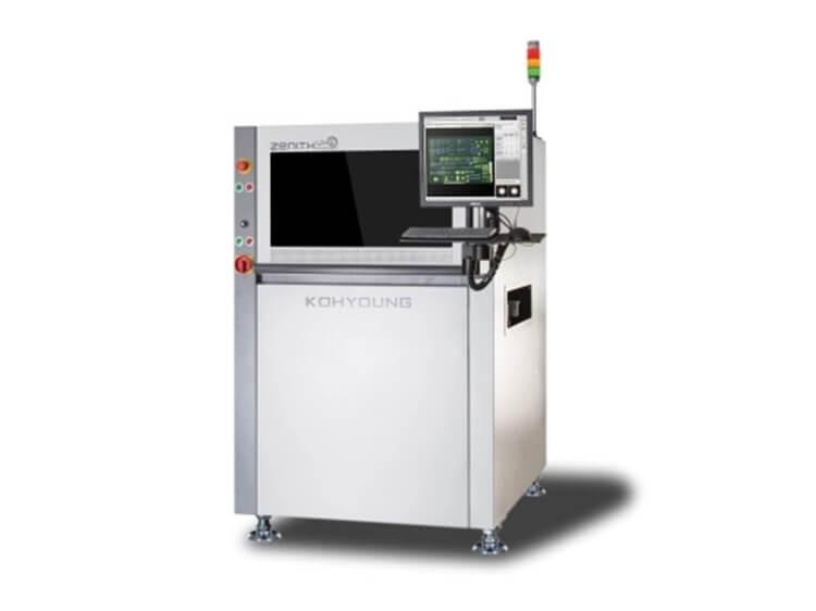
KOH YOUNG Zenith UHS 3D AOI Camera: 12M 15um Max PCB: 490 x 510 mm Weight: 600kg Dimension: 820x1265x1627 mm KOH YOUNG Zenith UHS 3D AOI KOH YOUNG Zenith UHS 3D AOI A model with 8 projections and an 8MPx camera. This model is very resistant t
New Equipment | Solder Paste Stencils
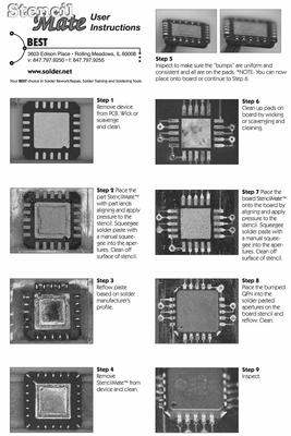
Simplify and Speed Up QFN and LGA device rework. StencilMate™ leadless device rework stencils make the process of reworking leadless devices such as QFNs and LGAs simple and fast. These adhesive-backed poyimide stencils are placed on to the bottom o
Electronics Forum | Mon Jul 22 13:19:31 EDT 2019 | davef
While we're are it, here's a link to a recent FORUM thread that talk's about BTC standoff height: https://smtnet.com/Forums/index.cfm?fuseaction=view_thread&CFApp=1&Thread_ID=21852&mc=9
Electronics Forum | Fri Jul 19 22:26:32 EDT 2019 | dhanish
Thanks Dave..What is the voids spec for QFN?This is another challenge with the QFN's

Used SMT Equipment | AOI / Automated Optical Inspection
OMRON AOI VT-S720-A MACHINE Hardware Configuration Image signal input unit Main unit Power supply Air Camera Illumination Image resolution Feed method Line height PCB carrier width adjustment Ambient operating temperature Ambient opera
Used SMT Equipment | AOI / Automated Optical Inspection
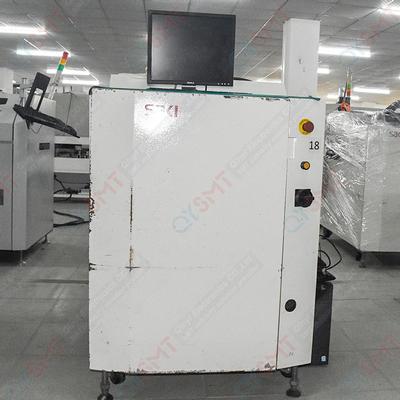
Saki BF-Frontier AOI System Model BF-Frontier Vintage: 12/2006 Board Thickness: 0.6 - 2.5mm, 24 - 100mils Board Warp: +/-2mm, 79mils PCB Clearance; Top: 40mm, 1.57in Bottom: 40mm, 1.57in Inspection Categories: Presence/Absence, Misalignment, Tomb sto
Industry News | 2012-01-10 19:20:12.0
IPC announced the winning research papers selected in the 2012 IPC International Academic Paper Competition.
Industry News | 2010-09-30 00:35:51.0
The new E revisions of IPC’s popular desk reference manuals, IPC-DRM-PTH, Through-Hole Solder Joint Evaluation Training & Reference Guide and IPC-DRM-SMT, Surface Mount Solder Joint Evaluation Training & Reference Guide have been released.
Technical Library | 2018-05-23 12:12:43.0
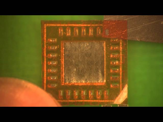
Driven by miniaturization, cost reduction and tighter requirements for electrical and thermal performance, the use of lead-frame based bottom-termination components (LF-BTC) as small-outline no-leads (SON), quad-flat no leads (QFN) packages etc., is increasing. However, a major distractor for the use of such packages in high-reliability applications has been the lack of a visible solder (toe) fillet on the edge surface of the pins: because the post-package assembly singulation process typically leaves bare copper leadframe at the singulation edge, which is not protected against oxidation and thus does not easily solder-wet, a solder fillet (toe fillet) does not generally develop.
Technical Library | 2015-06-11 21:20:29.0
The use of bottom terminated components (BTC) has become widespread, specifically the use of Quad Flat No-lead (QFN) packages. The small outline and low height of this package type, improved electrical and thermal performance relative to older packaging technology, and low cost make the QFN/BTC attractive for many applications.Over the past 15 years, the implementation of the QFN/BTC package has garnered a great amount of attention due to the assembly and inspection process challenges associated with the package. The difference in solder application parameters between the center pad and the perimeter pads complicates stencil design, and must be given special attention to balance the dissimilar requirements
The TR7500QE AOI offers high performance 3D solder and assembly inspection by combining the next generation multi-angle 2D and 3D technologies based on 4-way adaptive digital fringe pattern projection and 4 side view cameras. Latest inspection softwa
1st Place Machinery Inc. | http://www.firstplacemachinery.com/firstplace_asymtek1020.html
Asymtek 1020 Asymtek 1020 Dispenser Serial Number: X12367 Model Number: X-1020 (Dual Lane Option upgrade to X-1022) Year Jan 2007 DJ9000 Pump Head Windows XP Weight Scale Height Sensor The X-1020 system offers precise control over positioning accuracy using sealed glass linear encoders


