Industry Directory | Manufacturer
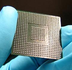
CVInc services advanced packaging. Placing solder bumps on single die, partial wafers, and complete wafers...we also offer RDL (redistribution) services in 5-7 working days. Our custom preforms are as small as 50um geometries.
Industry Directory | Consultant / Service Provider / Manufacturer
A Contract Manufacturing company specializing in Printed Circuit Board Assembly, Quick Turn Prototype Services, and Direct Fulfillment.
New Equipment | Rework & Repair Services
BGA Rework Services Offered BGA Remove and Placement Level Three Pad Repair Wire Add Trace Repair BGA Re-Balling BGA Inspection We Rework PBGA (Plastic Ball Grid Array) TBGA (Tape Ball Grid Array) uBGA (Micro BGA) CCGA (Ceramic Colum
600V *RO4350B *RO4003C Dielectric material & Stack up requirement FR-4(no copper): 0.05-3.2mm for option Prepreg type: 7628H(7630), 7628(43%), 7628(41%), 2116HR, 2116, 2113, 1080 and 1060 for option Copper
Electronics Forum | Mon Jun 01 16:48:16 EDT 2009 | stevezeva
Mika, Have you ever worked with a 3-row I/O QFN? QFN180 to be exact? Steve
Electronics Forum | Fri May 15 10:04:59 EDT 2009 | aj
Hi all, Is there any standard for percentage voiding on the center thermal pad on a QFN? We use the dot matrix array for paste to allow for outgassing etc, but we have had a couple of xray inspection "fails" for voiding on this pad , in or around 3
Industry News | 2011-09-14 12:04:43.0
The SMTA announced a session on QFN Assembly and Reliability will take place on Tuesday, October 18 during their annual conference, SMTA International, in Ft. Worth, Texas. Andrew Mawer of Freescale Semiconductor will chair the session and Viswam Puligandla, Ph.D., Nokia (Retired) will co-chair.
Industry News | 2018-10-18 08:40:47.0
Stencil aperture considerations for QFN chips
Technical Library | 2011-06-09 20:28:30.0
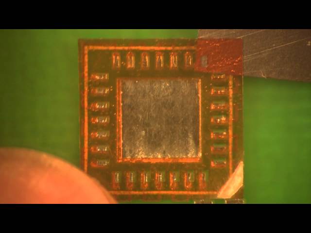
QFN Description: A QFN package is a QUAD-FLAT-NO LEAD device. This package is small and lightweight and has no leads (unlike a gull wing or J-leaded device). QFN’s have a thermal pad (paddle) on the bottom side of the part that offers heat dissipation and
Technical Library | 2012-10-18 21:58:51.0
First published in the 2012 IPC APEX EXPO technical conference proceedings. In this paper, we report on a comprehensive study regarding the morphology evolution and voiding of SnAgCu solder joints on the central pad of two different packages – QFN and an Agilent package called TOPS – on PCBs with a Ni/Au surface finish.
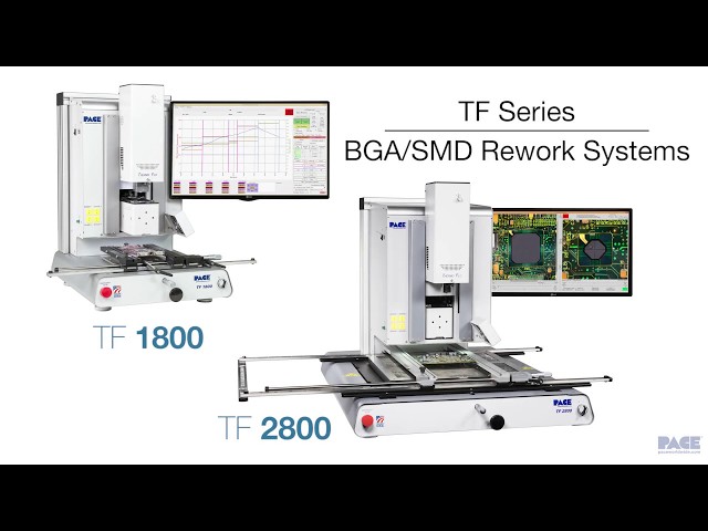
Enter PACE’s TF Series BGA/SMD Rework Systems. With its groundbreaking, patented Inductive-Convection Heating Technology, the TF Series top-side heater reaches the target temperature in just seconds for safe, rapid solder joint reflow in virtually an
Training Courses | | | PCB Rework and Hand Soldering Courses
The PCB rework and hand soldering courses courses cover techniques of rework and repair of PCBs, BGAs and other electronics assemblies, and teach fundamentals of soldering of electronics assemblies.
Training Courses | | | PCB Rework and Hand Soldering Courses
The PCB rework and hand soldering courses courses cover techniques of rework and repair of PCBs, BGAs and other electronics assemblies, and teach fundamentals of soldering of electronics assemblies.
Career Center | Sherman, Texas USA | Engineering,Production,Research and Development,Technical Support
SMT Packaging Engineer: Location: Texas - Sherman , TX Group: HVAL Degree Requirements: BS ME/ChemE/Materials The person in this position will have the ability to make very significant financial contributions to TI because this is a very critic
Career Center | Bangalore, India | Engineering,Maintenance,Production,Technical Support
SMT Stencil designing & Knowledge of full SMT process software known CAD/CAM -circuit CAM Pro 7.3,GC Power station, GCCAM Edit,Auto CAD, Fault finding of Electronic Boards & Servicing electronic machines.
The Morphology Evolution and Voiding of Solder Joints on QFN Central Pads with a Ni/Au Finish SMTnet Express October 19, 2012, Subscribers: 25598, Members: Companies: 9011, Users: 33828 The Morphology Evolution and Voiding of Solder Joints on QFN
SMTnet Express, June 11, 2015, Subscribers: 22,861, Members: Companies: 14,392 , Users: 38,338 Solder Paste Stencil Design for Optimal QFN Yield and Reliability B. Gumpert; Lockheed Martin Corporation The use of bottom terminated components (BTC
ASYMTEK Products | Nordson Electronics Solutions | https://www.nordson.com/en/divisions/dage/application/smt
. QFNs are very space efficient and are often used where the PCBA size must be minimal. QFN devices usually feature a large cooling pad underneath, ideal for applications where good thermal performance is required


