
Industry Directory | Consultant / Service Provider
PCB Electronics Manufacturing Automation Software for EMS, OEM & ODM manufacturers. Over 3000 customers worldwide!
Industry Directory | Manufacturer
An innovative thermal management company that is dedicated to address the thermal challenges that the electronics industry is facing.
New Equipment | Education/Training
In this One-Day class you will learn successful techniques to re-ball BGA Components. Both Lead and Lead Free Solder Balls will be covered. The student will have an opportunity to use and evaluate some of the most popular BGA rework fixtures on the
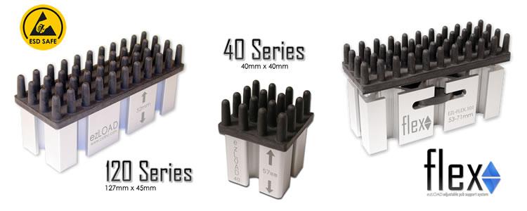
New Equipment | Board Handling - Pallets,Carriers,Fixtures
Count On Tools Inc., a leading provider of precision components and SMT spare parts, introduces the new ezLOAD PCB Support System. With the recent increase of densely populated double-sided circuit boards, COT recognized the need for more affordable
Electronics Forum | Mon Aug 28 17:54:59 EDT 2000 | Steve Thomas
We're trying out 0603 packages on some 0805 footprints (at this stage only on some test boards) since our vendor tells us the 0805's are going to be getting harder to get, and more expensive to pay for. I understand the IPC footprint for the two is
Electronics Forum | Mon Apr 01 12:07:25 EST 2002 | slthomas
* What material are you using? Loctite 3609 * What is your cure profile? In excess of the 90-120 seconds at 150C that Loctite recommends. * Dot dimensions and tip? 27g. conical tipped needle for the 0603's. I started with a 14 mil dot which loo

Used SMT Equipment | SPI / Solder Paste Inspection
PARMI/SPI SPIHS60 MACHINE PARMI HS60 (supreme) solder paste thickness tester SPI The SPI HS60 (supreme) series is the next generation fastest online solder paste inspection system on the market. The measurement speed at a resolution of 13x13um is
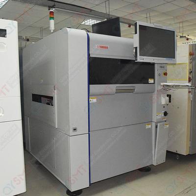
Used SMT Equipment | AOI / Automated Optical Inspection
YAMAHA AOI YSi-V MACHINE KLT-000 1. Model: Yamaha ysi-v 2. Target substrate: l610 x w560 (maximum) ~ l50 x w50 (minimum) & supports l750mm super long substrate (optional) 3. Resolution: visible light (red/green/blue) & infrared (infra-
Industry News | 2003-03-21 08:12:24.0
Tecan reckons it is consistently producing what may be regarded as the most efficient stencils in the world today.
Industry News | 2003-02-11 08:42:41.0
To Handle Outbound Logistics Projects for OEMs and to Gain Greater Insight into Their Customers' Requirements for Global Direct-order Fulfillment
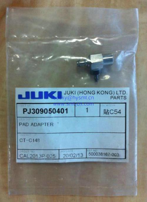
Parts & Supplies | SMT Equipment
JUKI PAD ADAPTER PJ309050401 PJ308060501 BRANCH PJ308065101 BRANCH PJ309040003 REDUCER 4-10 PJ309040004 CROSS JOINT PJ309040006 ELBOW PJ309040502 AIR BRANCH PJ309050401 PAD ADAPTER PJ309060002 IKEI TRIPLE 6-4 PJ309060005 DIFFERENT DIAMETER
Parts & Supplies | Turnkey Lines
ENGLISH KEY SHEET X02H84201 SOLENOILD VALVE ..N411VZ51-239 Cable SMA Male To SMA Male L:60cm/Brass Tubing SPF085 BEARING, BALL ..13155000 NUT ..X055903 Anvil cutter ..45575701 HEX. SOCKET HEAD CAP BOLT ..N51001733
Technical Library | 2020-08-27 01:22:45.0
Initially adopted internal specifications for acceptance of printed circuit boards (PCBs) used for wire bonding was that there were no nodules or scratches allowed on the wirebond pads when inspected under 20X magnification. The nodules and scratches were not defined by measurable dimensions and were considered to be unacceptable if there was any sign of a visual blemish on wire-bondable features. Analysis of the yield at a PCB manufacturer monitored monthly for over two years indicated that the target yield could not be achieved, and the main reasons for yield loss were due to nodules and scratches on the wirebonding pads. The PCB manufacturer attempted to eliminate nodules and scratches. First, a light-scrubbing step was added after electroless copper plating to remove any co-deposited fine particles that acted as a seed for nodules at the time of copper plating. Then, the electrolytic copper plating tank was emptied, fully cleaned, and filtered to eliminate the possibility of co-deposited particles in the electroplating process. Both actions greatly reduced the density of the nodules but did not fully eliminate them. Even though there was only one nodule on any wire-bonding pad, the board was still considered a reject. To reduce scratches on wirebonding pads, the PCB manufacturer utilized foam trays after routing the boards so that they did not make direct contact with other boards. This action significantly reduced the scratches on wire-bonding pads, even though some isolated scratches still appeared from time to time, which caused the boards to be rejected. Even with these significant improvements, the target yield remained unachievable. Another approach was then taken to consider if wire bonding could be successfully performed over nodules and scratches and if there was a dimensional threshold where wire bonding could be successful. A gold ball bonding process called either stand-off-stitch bonding (SSB) or ball-stitch-on-ball bonding (BSOB) was used to determine the effects of nodules and scratches on wire bonds. The dimension of nodules, including height, and the size of scratches, including width, were measured before wire bonding. Wire bonding was then performed directly on various sizes of nodules and scratches on the bonding pad, and the evaluation of wire bonds was conducted using wire pull tests before and after reliability testing. Based on the results of the wire-bonding evaluation, the internal specification for nodules and scratches for wirebondable PCBs was modified to allow nodules and scratches with a certain height and a width limitation compared to initially adopted internal specifications of no nodules and no scratches. Such an approach resulted in improved yield at the PCB manufacturer.
Technical Library | 2024-07-24 01:04:35.0
Quad Flat No Leads (QFN) package designs receive more and more attention in electronic industry recently. This package offers a number of benefits including (1) small size, such as a near die size footprint, thin profile, and light weight; (2) easy PCB trace routing due to the use of perimeter I/O pads; (3) reduced lead inductance; and (4) good thermal and electrical performance due to the adoption of exposed copper die-pad technology. These features make the QFN an ideal choice for many new applications where size, weight, electrical, and thermal properties are important. However, adoption of QFN often runs into voiding issue at SMT assembly. Upon reflow, outgassing of solder paste flux at the large thermal pad has difficulty escaping and inevitably results in voiding. It is well known that the presence of voids will affect the mechanical properties of joints and deteriorate the strength, ductility, creep, and fatigue life. In addition, voids could also produce spot overheating, lessening the reliability of the joints.
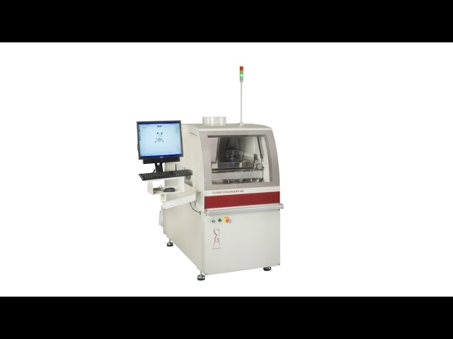
Flexible, in-line, modular selective soldering system Designed as a modular system, the Synchrodex range of in-line equipment offers the ultimate in flexibility with the ability to upgrade to high speed throughput when multiple modules are placed to
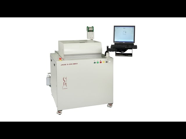
To see more about the Jade MKII Single Point Selective Soldering System visit Pillarhouse USA at: https://www.pillarhouse.co.uk/products/selective-soldering-handload/jade-mkii-handload Entry-level, single point selective soldering system Designed t
Training Courses | | | PCB Rework and Hand Soldering Courses
The PCB rework and hand soldering courses courses cover techniques of rework and repair of PCBs, BGAs and other electronics assemblies, and teach fundamentals of soldering of electronics assemblies.
Training Courses | | | PCB Rework and Hand Soldering Courses
The PCB rework and hand soldering courses courses cover techniques of rework and repair of PCBs, BGAs and other electronics assemblies, and teach fundamentals of soldering of electronics assemblies.
Events Calendar | Wed Apr 20 00:00:00 EDT 2022 - Wed Apr 20 00:00:00 EDT 2022 | ,
Virtual Course: Selection Criteria of Surface Finish for Next Generation PCB Technologies
Events Calendar | Mon Apr 12 00:00:00 EDT 2021 - Mon Apr 12 00:00:00 EDT 2021 | ,
Europe Chapter Webinar: Tombstoning Components during Reflow Soldering - Causes & Cures
Career Center | Wellsboro, Pennsylvania USA | Engineering
SMT PROCESS ENGINEER: (Wellsboro, PA) - Designs, defines and plans the manufacturing process. Specifies and directs installation of new processes. Plans equipment build schedules and monitors vendor progress. Defines and recommends equipment, methods
| https://www.eptac.com/webinars/damage-prevention-when-soldering-ceramic-chip-capacitors
. Add to this, the transition to lead free soldering materials, which have imposed more rigidity and reduced flexibility on solder joints, resulting in additional stress issues on these small devices
ASYMTEK Products | Nordson Electronics Solutions | https://www.nordson.com/en/divisions/industrial-coating-systems/application-solutions/powder-coating/automotive
. From relatively simple manual systems to those that are more sophisticated and automated, our technologies are used to coat aluminum and steel wheels, springs, brake pads, truck and bus frames, and trim


