Industry Directory | Manufacturer
A Manufacturer of High Quality, Precision, Automated Fluid Dispensing and Conformal Coating Systems, SMT Cover Tape Peel Tester and Lead Forming machines for through-hole component preparation.

Industry Directory | Equipment Dealer / Broker / Auctions
At ZJ-SMT, we provide premium SMT and PCB assembly equipment and components from leading brands such as Panasonic, Yamaha, Fuji, etc.

If you have boards requiring high tolerance mechanical dimension or odd shapes that traditional depaneling methods cannot handle. BEST Inc. provides laser depaneling services for printed circuit board manufacturers as well as EMS and OEMs. BEST’s nu

New Equipment | Rework & Repair Services
BEST offers contract PCB rework services. If you get in bind and need resources to perform difficult repairs or if the volume of work ahead of you is too extreme to get through in the deadline at hand then consider BEST PCB rework services. If you th
Used SMT Equipment | Conveyors
Nutek Open LIFO, XXL-size Type: NTM650SXXL Serial Nr.: 2012-0810E01 Year of Manufacture: 2013 Direction: Left to Right Transfer height: 900mm (+/-25mm) PCB size: 50 – 535mm (W)/ 80 -850mm (L) Product thickness: 0.60 – 1.60mm Component Height: Top: 30

Used SMT Equipment | AOI / Automated Optical Inspection
SAKI Desktop AOI BF18D-P40 Inspection Machine Substrate flatness: ±2mm Board size:50 * 60 - 250 * 330mm PCB thickness: 0.6mm - 2.5mm weight::30KG ■ Industry-Leading High Throughput Leading High Throughput The Alternate Color Digital Scanning
Industry News | 2016-08-25 17:56:34.0
GPD Global's advanced Precision Auger Pump retrofits into your dispensing system to provide excellent dispense control and repeatability. Precision Auger Pump Integration provides your process development with a broad range of functionality.
Industry News | 2024-04-06 00:43:25.0
Live demos at IPC APEX Expo 2024 – Booth 1504 – April 9-11, 2024, Anaheim, CA GRAND JUNCTION, CO USA -- April 2024 -- GPD Global – manufacturer of precision fluid dispensing systems for high-volume 24/7, low-volume/high-mix, and R&D production – will exhibit in Booth 1504 at IPC APEX EXPO 2024 on April 9-11 in the Anaheim Convention Center, CA.
Technical Library | 2007-02-01 10:08:40.0
The increased replacement of high lead count SMT devices with BGAs and other high ball count area array packages has brought increased challenges to PCB rework and repair. Often solder mask areas surrounding BGA pad areas are damaged when components are removed.
Technical Library | 2024-02-02 07:48:31.0
Maximizing Efficiency: The High-Speed SMT Line With Laser Depanelizer In today's rapidly evolving electronics manufacturing landscape, optimizing efficiency, cost-effectiveness, and precision remains paramount. Businesses engaged in producing industrial control boards, computer motherboards, mobile phone motherboards, and mining machine boards face ongoing challenges in streamlining production processes. The integration of expensive equipment strains budgets, making the creation of an efficient, cost-effective high-speed SMT line a daunting task. However, a solution exists that seamlessly combines these elements into a singular, high-performance, and cost-effective SMT line. Let's delve into the specifics. A Comprehensive High-Speed SMT Line Our innovative solution amalgamates two pivotal components: a cutting-edge SMT (Surface Mount Technology) production line and a laser cutting line equipped with a depanelizer. The SMT Production Line The high-speed SMT line comprises several essential components, each fulfilling a unique role in the manufacturing process: 1. PCB Loader: This initial stage involves loading boards onto the production line with utmost care. Our Board Loader prioritizes safety, incorporating various safety light curtains and sensors to promptly halt operations and issue alerts in case of any anomalies. 2. Laser Marking Machine: Every PCB receives a unique two-dimensional code or barcode, facilitating comprehensive traceability. Despite the high-temperature laser process potentially leading to dust accumulation on PCB surfaces, our dedicated PCB Surface Cleaner swiftly addresses this issue. 3. SMT Solder Paste Printer: This stage involves applying solder paste to the boards, a fundamental step in the manufacturing process. 4. SPI (Solder Paste Inspection): Meticulous inspections are conducted at this stage. Boards passing inspection proceed through the NG (No Good) Buffer Conveyor to the module mounters. Conversely, "No Good" results prompt storage of PCBs in the NG Buffer Conveyor, capable of accommodating up to 25 PCBs. Operators can retrieve these NG boards for rework after utilizing our specialized PCB Mis Cleaner to remove solder paste. 5. Module Mounters: These machines excel in attaching small and delicate components, necessitating precision and expertise in the module mounting process. 6. Standard Pick And Place Machines: The selection of these machines is contingent upon your specific BOM (Bill of Materials) list. 7. Pre-Reflow AOI (Automated Optical Inspection): Boards undergo examination for component quality at this stage. Detected issues prompt the Sorting Conveyor to segregate boards for rework. 8. Reflow Oven: Boards undergo reflow soldering, with our Lyra series reflow ovens recommended for their outstanding features, including nitrogen capability, flux recycling, and water cooling function, ensuring impeccable soldering results. 9. Post-Reflow AOI: This stage focuses on examining soldering quality. Detected defects prompt the Sorting Conveyor to segregate boards for further inspection or rework. Any identified defects are efficiently addressed with the BGA rework station, maintaining the highest quality standards. 10. Laser Depanelizer: Boards advance to the laser depanelizer, where precision laser cutting, often employing green light for optimal results, ensures smoke-free, highly accurate separation of boards. 11. PCB Placement Machine: Cut boards are subsequently managed by the PCB Placement Machine, arranging them as required. With this, all high-speed SMT line processes are concluded. Efficiency And Output This production line demonstrates exceptional productivity when manufacturing motherboards with approximately 3000 electronic components, boasting the potential to assemble up to 180 boards within a single hour. Such efficiency not only enhances output but also ensures cost-effectiveness and precision in your manufacturing processes. At I.C.T, we specialize in crafting customized SMT production line solutions tailored to your product and specific requirements. Our equipment complies with European safety standards and holds CE certificates. For inquiries or to explore our exemplary post-sales support, do not hesitate to contact us. The I.C.T team is here to elevate your electronics manufacturing to new heights of efficiency and cost-effectiveness.

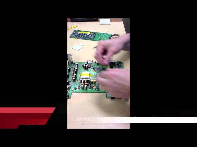
These are the instructions for the BEST Heatshields(TM) an effective, high tech simple way to shield heat sensitive components during reflow/rework. This ceramic-based non-woven material, when properly deployed, will protect components so that they d
Training Courses | ON DEMAND | | PCB Rework and Hand Soldering Courses
The PCB rework and hand soldering courses courses cover techniques of rework and repair of PCBs, BGAs and other electronics assemblies, and teach fundamentals of soldering of electronics assemblies.
Training Courses | ON DEMAND | | PCB Rework and Hand Soldering Courses
The PCB rework and hand soldering courses courses cover techniques of rework and repair of PCBs, BGAs and other electronics assemblies, and teach fundamentals of soldering of electronics assemblies.
Events Calendar | Sun Apr 11 18:30:00 UTC 2021 - Sun Apr 11 18:30:00 UTC 2021 | ,
Europe Chapter Webinar: Tombstoning Components during Reflow Soldering - Causes & Cures
Events Calendar | Wed Jun 07 18:30:00 UTC 2023 - Wed Jun 07 18:30:00 UTC 2023 | ,
SMTA Workforce Development Webinar: PCB Design Courses and Careers in PCB Design
Career Center | San Jose, California USA | Engineering
Headquartered in San Jose, as leading PC component distributor and rank #5 DRAM manufacturer in the worldwide, Ma Labs Inc. has specialized in memory modules since 1985. We provide a full range of memory modules from RDRAM, DDR, SD-RAM, SO-DIMM and F
Career Center | Nashville, North Carolina USA | Production
MUST BE WILLING TO BECOME FULLY VACCINATED FOR COVID-19, OR QUALIFY FOR A RECOGNIZED EXEMPTION, TO WORK AT ACDI IF GOVERNMENT CONTRACTOR REGULATIONS ARE UPHELD. OUR COMPANY What we do day-in and day-out has a lasting, meaningful impact across man
Career Center | , Israel | Engineering,Maintenance,Technical Support
I was born on June , 1972 in Khmelnitsky city , Ukraine . I am male. From 1979 to 1987 I was studying at secondary school #7, having finished which I entered the Technical College of Khmelnitsky in specialty Machine Tools with Computer Numeric Contr
Career Center | , Gjirokaster Philippines | Engineering,Production,Quality Control,Research and Development,Technical Support
TEST Engineer FOXCONN(Hon Hai Precision Ind., Ltd., Co)-formerly AMBIT Microsystems Co. Inc. Research and Development Center 5F-1 No. 5, Hsin Ann Road, Science-Based Industrial Park, Hsinchu City, Taiwan, R.O.C. General Job Functions: PCBA Testing u
SMTnet Express, October 13, 2022, Subscribers: 24,986, Companies: 11,630, Users: 27,497 █ Electronics Manufacturing Technical Articles Effects of PCB Substrate Surface Finish and Flux on Solderability of Lead-Free SAC305 Alloy
Imagineering, Inc. | https://www.pcbnet.com/blog/understanding-the-pcb-fabrication-process-from-design-to-delivery/
Understanding the PCB Fabrication Process: From Design to Delivery Skip to main content Resources Support Contact Us FAQs Live Chat My Account 847-806-0003 Menu PCB Capabilities Fabrication Technology Roadmap Materials Available HDI
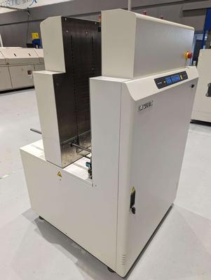
GPD Global | https://www.gpd-global.com/co_website/pdf/lead-former/CF8-User-Guide-801-1-07.pdf
. Ignore all references to Stations 4 & 5 (they are not present on the CF-15). 2. Roller or dimpling dies are not applicable. 3. No crimping on the component leads is performed


