Industry Directory | Manufacturer
PVA TePla Analytical Systems, a company that designs and manufactures advanced Scanning Acoustic Microscopes for both laboratory and production environments
Industry Directory | Consultant / Service Provider / Manufacturer
Designer & Manufacturer of Acoustic Microscopes for Nondestructive Component Inspection.
New Equipment | Test Equipment
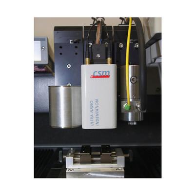
THE NEW GENERATION OF NANOINDENTER CSM Instruments has introduced a new nano range high resolution nanoindenter with ultra low thermal drift. When used per ISO 14577 test methods the Ultra Nano Hardness Tester will provide the most accurate data of
Used to inspection materials which do not admit x-ray penetration (e.g. ceramics). Also used in device-level inspection for defects and counterfeit detection.
Used SMT Equipment | Semiconductor & Solar
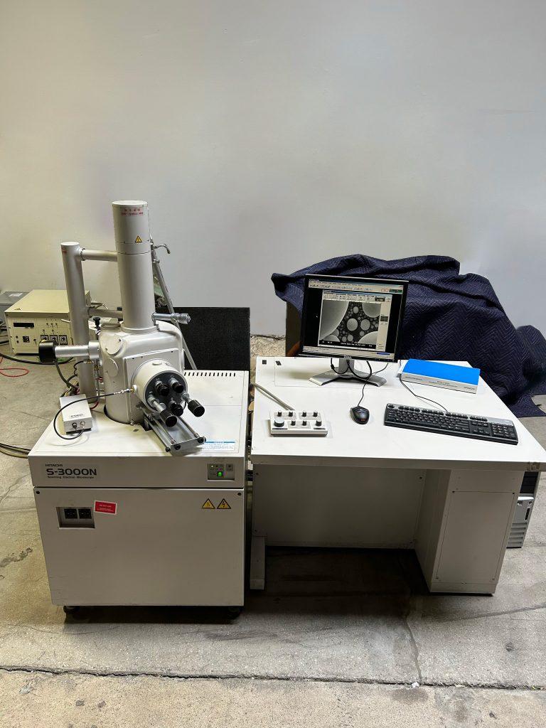
HITACHI S-3000-N Scanning Electron Microscope (SEM) Not sure of vintage! Full specifications upon request. https://www.karenmadison.com/hitachi-s-3000-n-scanning-electron-microscope-sem/
Used SMT Equipment | Semiconductor & Solar
Kulicke & Soffa ConnX Plus Wire Bonders High Speed Wire Bonder Ball Bonder **NOT LED** 7 available Vintage: 2013 & 2014 Available Extra Large Bond Area: 56mm x 80mm High Speed X-Y-Z Motion Control System +/- 3.0 μm Accuracy CCD V
Industry News | 2020-09-17 12:23:10.0
Talk to the experts and see demonstrations of the latest equipment for test and inspection, fluid dispensing, and plasma treatment in one booth, #I2716
Industry News | 2014-05-14 16:54:20.0
A newly released training video, DVD-166C, “Counterfeit Components” from IPC — Association Connecting Electronics Industries®, explains not only how counterfeit components find their way into the supply chain, but more important, how to detect fraudulent devices during visual inspection.
Technical Library | 2017-06-15 00:44:19.0
Ceramics packages are being used in the electronics industry to operate the devices in harsh environments. In this paper we report a study on acoustic imaging technology for nondestructively inspecting underfill layers connecting organic interposers sandwiched between two ceramics substrates.First, we inspected the samples with transmission mode of scanning acoustic tomography (SAT) system, an inspection routine usually employed in assembly lines because of its simpler interpretation criteria: flawed region blocks the acoustic wave and appears darker. In this multilayer sample, this approach does not offer the crucial information at which layer of underfill has flaws. To resolve this issue, we use C-Mode Scanning in reflection mode to image layer by layer utilizing ultrasound frequencies from 15MHz to 120MHz. Although the sample is thick and contains at least 5 internal material interfaces, we are able to identify defective underfill layer interfaces.
Technical Library | 2021-09-21 20:36:45.0
The present paper gives an overview of surface failures, internal nonconformities and solders joint failures detected by microscopic analysis of electronic assemblies. Optical microscopy (stereomicroscopy) and Fourier-Transform- Infrared (FTIR) microscopy is used for documentation and failure localization on electronic samples surface. For internal observable conditions a metallographic cross-section analysis of the sample is required. The aim of this work is to present some internal and external observable nonconformities which frequently appear in electronic assemblies. In order to detect these nonconformities, optical microscopy, cross section analysis, FTIR-microscopy and scanning electron microscopy with energy dispersive spectrometry (SEM-EDS) were used as analytical techniques.

Sonix Acoustic Microscope C-SAM #3 UHR2001 Price: $4,500.00 Model Number : C-SAM #3 Serial Number : UHR2001 Manufacturer: Sonix Dimensions: 440x40x50 Condition: Used - Unit powers up and appears to be functional. - Possibly missing transduc
![[SEC] SEM(Scanning Electron Microscope) SNE 4500M Plus Premium Version of Highest-end](https://img.youtube.com/vi/C9ny0wTR8mY/sddefault.jpg)
#SEM#SEC#??????? Model: SNE-4500M Plus (A) / (B) Resolution: 5nm (30kV, SE Image) Magnification: 30x~150,000x Detector: Secondary Electron(SE) / Backscattered Electron(BSE) Vacuum: High / Low Stage: X,Y, Z, R, T : Fully motorized Navigation mode wi
Training Courses | | | Other Courses
Other courses related to electronics manufacturing and assembly
Events Calendar | Thu Sep 17 18:30:00 UTC 2020 - Thu Sep 17 18:30:00 UTC 2020 | ,
Defect Detection for Advanced Wafer and Package Devices
Career Center | Milpitas, California USA | Engineering,Production,Quality Control,Research and Development,Technical Support
Winslow Automation, Inc. (aka Six Sigma), an industry leader in electronic component interconnect technology & related test and failure analysis services, is seeking individuals specializing in materials lab testing to join our team. We have openin
Career Center | Rochester, New York USA | Engineering
I have done my undergraduate studies in Mechanical Engineering. I am pursuing my Master's Program in Electronics Packaging. I am currently working as a Research Assistant for RIT-CEMA (Center for Electronics Manufacturing and Assembly). My research
Career Center | , | Engineering,Production,Quality Control,Research and Development
WORK EXPERIENCE Hutchinson Technology Incorporated, MN Feb.2006-Present Process Development Engineering Co-op �Study of voids generation in solder ball bonded Cu substrate with Ni/Au metallization. �Diffusion & Intermetallic growth study in sold
ASCEN Technology | https://www.ascen.ltd/Blog/Gif/list_57_3.html
machine.uses to manual welding of earbands/earloops.Connect mask with ear loop well by the high-frequency elastic vibration of acoustic system
Heller Industries Inc. | https://hellerindustries.com/wp-content/uploads/2018/07/pan_APEX06.pdf
). The fracture surfaces have been studied using a scanning electron microscopy (SEM) with energy dispersive spectroscopy (EDS). Introduction The increasing awareness of health risk associated with lead (Pb


