
Industry Directory | Other / Consultant / Service Provider / Media / Publisher / Online Resource
PCB Libraries' "Footprint Expert" suite uses CAD LEAP(tm) Technology to greatly simplify footprint and 3D STEP model creation; it is used by tens of thousands of PCB designers and engineers all over the world.

Industry Directory | Other / Consultant / Service Provider / Manufacturer
ScanCAD is an industry leader in inspection, measurement, process control and reverse engineering. Our solutions support OEM's, manufacturers, stencil fabricators, repair depots, and others in optimizing quality and yield.
ProntoPLACE used by electronics manufacturers will quickly program your surface mount SMT and thru-hole assembly equipment. In minutes Unisoft ProntoPLACE software translates CAD or Gerber and Bill of Materials (BOM) files into real reference desig
ProntoVIEW-MARKUP is assembly CAD Viewer & Gerber Viewer software used by electronics manufacturers to quickly find components, pin, shorts between traces, etc. ProntoVIEW-MARKUP is also a redline tool that allows annotation of the assembly to creat
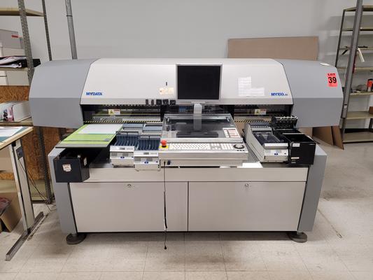
Used SMT Equipment | Pick and Place/Feeders
For sale via online auction, unreserved, everything must goAuction ends August 25th from 10am - Online bankruptcy auction for the former assets of Ampere Inc. in La Pocatiere, Quebec. Auction Web Site: https://www.bidspotter.com/en-us/auction-catalo
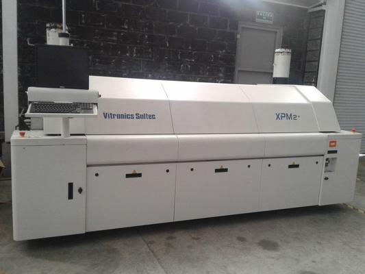
Used SMT Equipment | Soldering - Reflow
Heating zones: 5 Cooling zones: 2 Total heating length: 66 in. Total cooling length: 26 in. Total process length: 127 in. Total on /off load length: 11 in. Overall system length: 138.5 in. Overall system width: 52 in. Overall system height: 5
Industry News | 2003-02-04 08:49:40.0
John Was the Product Manager for Orcad's Schematic Capture and PCB Layout Programs from 1994 to 2001
Industry News | 2003-05-06 09:05:12.0
New Schematic Capture and Simulation Software Delivers Innovative Features and the Industry�s Best Price/Performance
Technical Library | 2015-04-08 11:10:47.0
An electronic schematic describes the electrical connectivity of a piece of equipment or an entire system. It is made up of symbols that represent individual components and contains electrical and mechanical information and their related connectivity, along with other important data. Information contained within the schematic is packaged into a printed circuit board (PCB) where the mechanical footprint is placed onto the board and connectivity information is graphically displayed. The more accurate the information contained in the schematic is and the clearer it is presented, the more it contributes to a robust printed circuit board.
Technical Library | 2018-02-01 00:31:48.0
This paper briefly summarizes the technologies underpinning the evolution in electrical system diagnosis and repair, which include schematic layout automation using prototypes and rule-based styling, instant language translation, 2D/3D view links with schematics, interactive diagnostic procedures, and dynamically-generated signal-tracing diagrams. These technologies empower after-sales service teams with state-of-the-art capabilities, which not only reduce costs but also improve brand quality in the eyes of its customers.

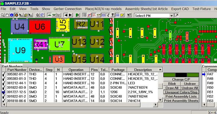
www.unisoft-cim.com/pcbplace.htm - The ProntoPLACE module from Unisoft is used by electronics manufacturers to generate the necessary programs for automatic PCB assembly machines in minutes. ProntoPLACE programs most popular surface mount (SMT) place

www.unisoft-cim.com/pcbtest.htm - In minutes the Unisoft ProntoTEST-FIXTURE software translates CAD & BOM files into real reference designators, netlists, X/Y component pin geometries, values, tolerances, part numbers, etc. This data is used by Test
Training Courses | | | IPC Designer Certification CID
The Certified IPC Designer CID (Certified Interconnect Designer) course is the industry's premier professional development program for experienced PCB design professionals.
Training Courses | | | IPC Designer Certification CID
The Certified IPC Designer CID (Certified Interconnect Designer) course is the industry's premier professional development program for experienced PCB design professionals.
Career Center | Fremont, California USA | Engineering
Interprets electrical design requirements and uses Allegro design tool to create original PCB layouts, detailed fab drawings, schematics, and other design files. Work with HW design engineer to make sure PCB layout meet PCB design requirements.
Career Center | Fremont, California USA | Engineering
Job Description: • Has full ownership of HW design and release including HW specification creation, schematic generation, PCB layout, board bring up, and design verification. • Complete PCB design schematic using Orcad capture. • Complete HW desig
Career Center | NEW DELHI, India | Technical Support
I am having almost 20 years of experience in the field of electronics repairs domestic & industrial, able to work on any circuit and PCB without any schematic or diagram. I have all the records and certifications with me and fully c
Career Center | Wabash, Indiana USA | 2001-02-14 01:57:43.0
4 years experiance in: Schematics Soldering Circuit Board Repair Electronics Troubleshooting Multi-Meter Oscilliscope Network Analyzer RF Transmitters RF Recievers Antennas Maintenance Scheduling Composing and implementing training plans
Imagineering, Inc. | https://www.pcbnet.com/blog/how-can-a-printed-circuit-board-help-you-test-a-circuit-board-schematic/
How Can a Printed Circuit Board Help You Test a Circuit Board Schematic? Skip to main content Resources Support Contact Us FAQs Live Chat My Account 847-806-0003 Menu PCB Capabilities Fabrication Technology Roadmap Materials Available HDI Tolerances Certifications
| https://unisoft-cim.com/view-markup_troubleshooting_netlist-and-blinking-of-pins-on-net.html
& Fixture GERBER Translations Other Services Testimonials Overview Pricing Contact Us NETLIST Window and Blinking of All Pins on the Selected Net Easier drill down to component pins, trace runs and schematic


