Industry Directory | Consultant / Service Provider / Manufacturer
Creative Hi-Tech is an ISO 9001:2008 registered and IPC-A-610-D compliant company providing high quality circuit board assemblies for varied industrial applications.
New Equipment | Rework & Repair Equipment
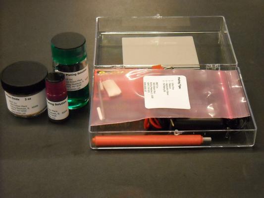
The BEST Gold Contact Replating Kit includes the tools you need for fast replating and modification of circuit contacts. Edge contacts may require replating if they are contaminated with solder or become scratched during handling or do not meet the m
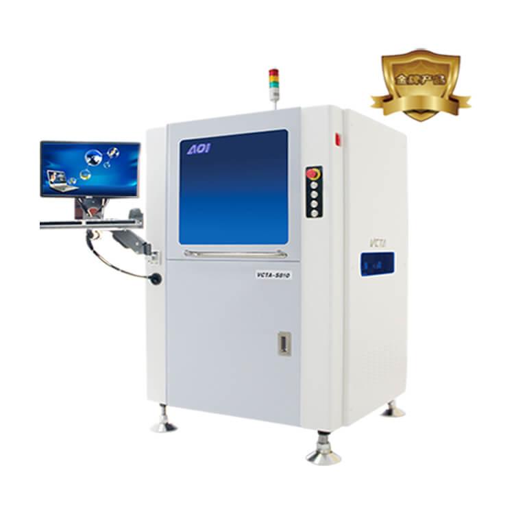
http://www.flason-smt.com/product/Online-AOI-Machine.html Online AOI Machine S810 Inspection Component: 01005 chip PCB size::50×70mm-510×460mm Dimension:1000mm×960mm×1600mm Weight: 710kg Product description: Online AOI
Used SMT Equipment | AOI / Automated Optical Inspection
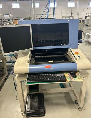
Mirtec MV-3L PCB AOI MACHINE IS IN GOOD WORKING CONDITION AND CAN BE DEMO'D IN PERSON OR VIRTUALLY! SN: 13100524-0524 DOM: 24 MAY 20102D InspectionPower: 85-264V / 4.4A / 50-60 HzINSPECTION AREA: 450 x 400 mmINSPECTION ITEMS: Lifted Lead, Lifted Comp
Used SMT Equipment | AOI / Automated Optical Inspection
2011 MIRTEC MV-3L PCB AOI MACHINE IS IN GOOD WORKING CONDITION AND CAN BE DEMO'D IN PERSON OR VIRTUALLY! SN: 13110930-0839 DOM: 30 SEP 2011 2D Inspection Power: 85-264V / 4.4A / 50-60 Hz INSPECTION AREA: 450 x 400 mm INSPECTION ITEMS:&n
Industry News | 2018-10-18 08:00:40.0
SMT solder joint quality and appearance inspection process
Industry News | 2018-10-18 08:01:00.0
SMT solder joint quality and appearance inspection process
Technical Library | 2020-08-27 01:22:45.0
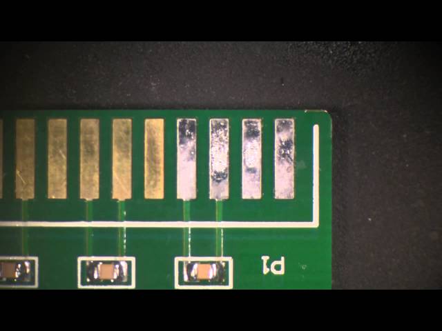
Initially adopted internal specifications for acceptance of printed circuit boards (PCBs) used for wire bonding was that there were no nodules or scratches allowed on the wirebond pads when inspected under 20X magnification. The nodules and scratches were not defined by measurable dimensions and were considered to be unacceptable if there was any sign of a visual blemish on wire-bondable features. Analysis of the yield at a PCB manufacturer monitored monthly for over two years indicated that the target yield could not be achieved, and the main reasons for yield loss were due to nodules and scratches on the wirebonding pads. The PCB manufacturer attempted to eliminate nodules and scratches. First, a light-scrubbing step was added after electroless copper plating to remove any co-deposited fine particles that acted as a seed for nodules at the time of copper plating. Then, the electrolytic copper plating tank was emptied, fully cleaned, and filtered to eliminate the possibility of co-deposited particles in the electroplating process. Both actions greatly reduced the density of the nodules but did not fully eliminate them. Even though there was only one nodule on any wire-bonding pad, the board was still considered a reject. To reduce scratches on wirebonding pads, the PCB manufacturer utilized foam trays after routing the boards so that they did not make direct contact with other boards. This action significantly reduced the scratches on wire-bonding pads, even though some isolated scratches still appeared from time to time, which caused the boards to be rejected. Even with these significant improvements, the target yield remained unachievable. Another approach was then taken to consider if wire bonding could be successfully performed over nodules and scratches and if there was a dimensional threshold where wire bonding could be successful. A gold ball bonding process called either stand-off-stitch bonding (SSB) or ball-stitch-on-ball bonding (BSOB) was used to determine the effects of nodules and scratches on wire bonds. The dimension of nodules, including height, and the size of scratches, including width, were measured before wire bonding. Wire bonding was then performed directly on various sizes of nodules and scratches on the bonding pad, and the evaluation of wire bonds was conducted using wire pull tests before and after reliability testing. Based on the results of the wire-bonding evaluation, the internal specification for nodules and scratches for wirebondable PCBs was modified to allow nodules and scratches with a certain height and a width limitation compared to initially adopted internal specifications of no nodules and no scratches. Such an approach resulted in improved yield at the PCB manufacturer.
BEST Inc master instructor Norman Mier demonstrates how to replate gold fingers using the BEST gold contact replating kit. In this video he demonstrates how to repair, prepare and replate the finger using a gold replating solution. If you want to lea
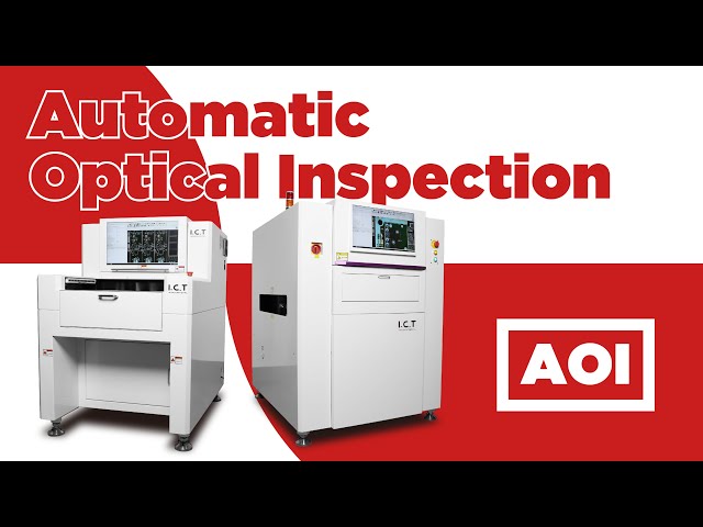
I.C.T Provide SMT Production Line solutions with Automated Optical Inspection (AOI) AOI is short for Automated Optical Inspection, which is widely used in the electronics industry to check the appearance of PCBA assembly at the back end of the cir
Career Center | Racine, Wisconsin USA | Engineering
Cree currently has a job vacancy for an SMT Process Technician in our Lighting Manufacturing facility in Racine, Wisconsin. Summary: This person will be a primary contributor to the startup of a new SMT production line for LED PCB Assembly. This
Career Center | Milwaukee, Wisconsin USA | Engineering
Cree Lighting, A company of IDEAL INDUSTRIES, is an LED lighting pioneer known for being first – first to bring LED lighting to the masses, first to deliver no compromise white light, and first to offer a sensor-integrated intelligent lighting
requiring regeneration from scratch to address very
Imagineering, Inc. | https://www.pcbnet.com/blog/pcb-equipment-101-what-equipment-is-used-to-pcb-assembly/
PCB Assembly Equipment List: What Is Used to Manufacture PCB? Skip to main content Resources Support Contact Us FAQs Live Chat My Account 847-806-0003 Menu PCB Capabilities Fabrication Technology Roadmap Materials Available HDI Tolerances Certifications
| https://www.eptac.com/blog/how-to-safeguard-against-counterfeit-components
: The easiest method to start with is a visual inspection of your components. Look for indicators such as sanding, scratches, mismatched paint, or inconsistencies in texture. Electrical Testing


