
Industry Directory | Consultant / Service Provider / Equipment Dealer / Broker / Auctions / Manufacturer's Representative / Training Provider
Products, services, training & consulting for the assembly, rework & repair of electronic assemblies. BGA process experts. Manufacturers Rep, Distributor & Service Provider for Seamark/Zhuomao and Shuttle Star BGA Rework Stations.
Industry Directory | Manufacturer
CVInc services advanced packaging. Placing solder bumps on single die, partial wafers, and complete wafers...we also offer RDL (redistribution) services in 5-7 working days. Our custom preforms are as small as 50um geometries.

Flux Free Formic Reflow Reflow in Formic Acid Vapor Heller has designed and built an production ready horizontal reflow oven for formic acid vapor. This new oven has been designed to meet Semi S2/S8 safety standards (including toxic gases). Form
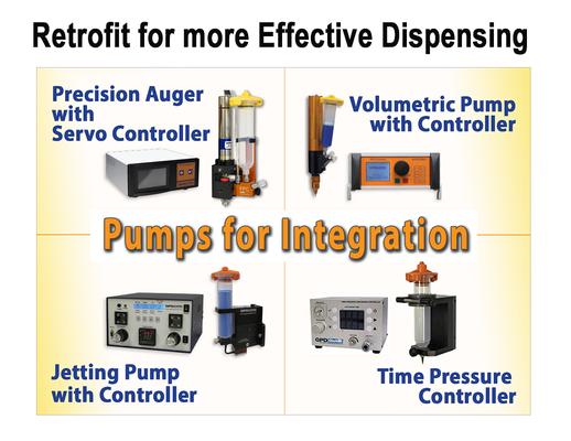
Retrofit existing system with Innovative Dispensing Technology for Excellent Dispense Control and Repeatability Advanced pump technologies available for retrofitting include: True Volumetric Pump, Precision Auger Pump, Simplified Jetting Pump and Ti
Electronics Forum | Thu Jan 14 23:49:00 EST 1999 | Wirat Sriamonkitkul
I saw the problem of void in solder bump or in lead less component or some BGA. But I didn't have standard specification of that void is accept or reject? Do any body have the better idea or suggestion of the criteria ? Thank you, Wirat S. / Jan 15
Used SMT Equipment | Screen Printers
Substrate processing: Maximum substrate size (XxY): 609.6mmx508mm(24”x20”) For circuit boards larger than 20”, special fixtures are required Minimum substrate size (XxY): 50.8mmx50.8mm(2”x2”)
Used SMT Equipment | Semiconductor & Solar
Bondtester by DAGE, in good condition. DAGE Series 4000 Bondtester product information. The 4000 bondtester is multipurpose, capable of performing all pull and shear applications. The 4000 bondtester can be configured as a simple bond wire pull
Industry News | 2013-08-15 20:58:22.0
Heller Industries announced today that they have entered into a joint development agreement with International Business Machines Corporation (NYSE: IBM), to collaborate on the development of fluxless mass reflow furnace equipment and process for high volume manufacturing. The fluxless process utilizes gas phase formic acid to replace standard fluxing agents, and eliminates the need for pre-reflow fluxing and post-reflow flux cleanup steps.
Industry News | 2016-07-16 13:32:29.0
Advanced dispense technology is available for integration into your dispensing system. Continuously Volumetric, drip-and-drool free dispense technology can now be retrofitted into your dispense robot. GPD Global's Volumetric PCD pumps ensure the success of applications like underfill, LED encapsulation, solder mask, silicones, conductive ink, conformal coatings, and more. Improve your throughput and yields by retrofitting a Volumetric PCD Pump into your dispense system to simplify the dispense process.
Technical Library | 2023-01-17 17:58:36.0
Heterogeneous integration has become an important performance enabler as high-performance computing (HPC) demands continue to rise. The focus to enable heterogeneous integration scaling is to push interconnect density limit with increased bandwidth and improved power efficiency. Many different advanced packaging architectures have been deployed to increase I/O wire / area density for higher data bandwidth requirements, and to enable more effective die disaggregation. Embedded Multi-die Interconnect Bridge (EMIB) technology is an advanced, cost-effective approach to in-package high density interconnect of heterogeneous chips, providing high density I/O, and controlled electrical interconnect paths between multiple dice in a package. In emerging architectures, it is required to scale down the EMIB die bump pitch in order to further increase the die-to-die (D2D) communication bandwidth. Aa a result, bump pitch scaling poses significant challenges in the plated solder bump reflow process, e.g., bump height / coplanarity control, solder wicking control, and bump void control. It's crucial to ensure a high-quality solder bump reflow process to meet the final product reliability requirements. In this paper, a combined formic acid based fluxless and vacuum assisted reflow process is developed for fine pitch plated solder bumping application. A high-volume production (HVM) ready tool has been developed for this process.
Technical Library | 2013-04-11 15:43:17.0
With the explosion of growth in handheld electronics devices, manufacturers have been forced to look for ways to reinforce their assemblies against the inevitable bumps and drops that their products experience in the field. One method of reinforcement has been the utilization of underfills to "glue" certain SMDs to the PCB. Bumped SMDs attached to the PCB with a no-clean soldering process offer the unavoidable scenario of the underfill coming in contact with a flux residue. This may or may not create a reliability issue... First published in the 2012 IPC APEX EXPO technical conference proceedings
Nano-copper sintering in formic acid vapor.

http://www.gpd-global.com No drip no drool across a wide range of fluid viscosities (low-to-mid and low-to-high). No manual adjustment to compensate for pump variability. Truly Volumetric PCD Pumps for total control of dispensing fluids. Ability to
Training Courses | | | PCB Rework and Hand Soldering Courses
The PCB rework and hand soldering courses courses cover techniques of rework and repair of PCBs, BGAs and other electronics assemblies, and teach fundamentals of soldering of electronics assemblies.
Training Courses | | | PCB Rework and Hand Soldering Courses
The PCB rework and hand soldering courses courses cover techniques of rework and repair of PCBs, BGAs and other electronics assemblies, and teach fundamentals of soldering of electronics assemblies.
Career Center | Philadelphia, New Jersey USA | Sales/Marketing
LOCATION BASE SALARY USA - NJ - Central USA - NJ - Southern USA - PA - Philadelphia $67000 - 73000 Another $50K to $70K in commissions based on plan COMPANY BRIEF My client is a leading supplier of automated broadband communications assembly e
Career Center | Brookfield, Wisconsin USA | Engineering
SR. ENGINEER � SENSORS -- $60-$80K Company: Well established controls manufacturer that has seen steady growth over the past several years. This company has a history of anticipating and successfully capitalizing on new market needs. Being one of t
Career Center | , District of Columbia | Engineering,Management,Production,Sales/Marketing
• Strong technical leadership and decision-making skills; strong verbal and written communication skills to provide clear, crisp direction for key issue resolution; and good team skills to facilitate cross-functional cross -site team effectiveness.
Career Center | , | Engineering,Production
Project Management, SMT Process Engineering
Featured Article Return to Front Page Soldering Technolo
SMTnet Express, April 21, 2022, Subscribers: 25,664, Companies: 11,565, Users: 27,188 Deep Learning Based Defect Detection for Solder Joints on Industrial X-Ray Circuit Board Images Quality control is of vital importance during
GPD Global | https://www.gpd-global.com/lead-free-solder-paste-dispensing.php
(solder sphere diameter) in many ways defines the smallest dot that can be dispensed. Table below shows recommended dot size for several paste types
Imagineering, Inc. | https://www.pcbnet.com/blog/identifying-and-correcting-solder-bridge-defects/
– with the push towards miniaturization and faster production speeds, solder bridge defects are an extremely problematic road bump that have become increasingly common


