
Industry Directory | Consultant / Service Provider / Media / Publisher / Online Resource / Other
PCB Libraries' "Footprint Expert" suite uses CAD LEAP(tm) Technology to greatly simplify footprint and 3D STEP model creation; it is used by tens of thousands of PCB designers and engineers all over the world.
SMT Plus offers online and onsite technical training in addition to selling technical publications for SMT design and manufacturing. SMT Plus is a leader in supplying land pattern libraries to the industry.
New Equipment | Rework & Repair Services
BGA Reballing and Solder Bumping for all types of SMD's Lead, Lead Free and Solder Alloy Conversion. Package types include but are not limited to: PBGA (Plastic Ball Grid Array) TBGA (Tape Ball Grid Array) uBGA (Micro BGA) CCGA (Ceramic Colum
New Equipment | Education/Training
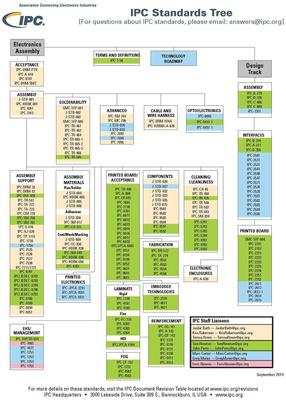
IPC standards, the results of industry consensus and collaboration, are respected throughout the whole world. Using IPC standards allows manufacturers, customers and suppliers to speak the same language. IPC standards are used by the electronics
Electronics Forum | Wed Jul 03 14:08:10 EDT 2002 | gbriceno
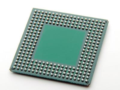
I' designing a PCB with SMD components to optimize the land patterns for wave soldering. I find that the IPC-SM-782 land patterns are not robust enough for wave soldering, yielding ramdom skips and bridges. This PCB will also give me insight on sha
Electronics Forum | Wed Jul 03 15:58:16 EDT 2002 | davef
Your thinking is correct. Wave soldering pads that were designed for reflow can create problems: * Large pads used for reflow [too much solder] can create reliability problems. * Bridging [too much solder] creates rework. * Skipping & shadowing from
Industry News | 2010-07-22 22:37:02.0
IPC — Association Connecting Electronics Industries® has released the B revision of IPC-7351, Generic Requirements for Surface Mount Design and Land Pattern Standard. The leading industry standard for surface mount land pattern design and layout, IPC-7351B provides designers and printed board fabricators with updated guidance on requirements of land pattern geometries used for the surface attachment of electronic components, as well as surface mount design recommendations for achieving the best possible solder joints.
Industry News | 2013-05-20 16:19:35.0
IPC – Association Connecting Electronics Industries® has teamed up with PCB Libraries, Inc.
Technical Library | 2018-10-24 18:04:12.0
Polymer Thick Film (PTF)-based printed electronics (aka Printed Electronics) has improved in durability over the last few decades and is now a proven alternative to copper circuitry in many applications once thought beyond the capability of PTF circuitry. This paper describes peak performance and areas for future improvement.State-of-the-art PTF circuitry performance includes the ability to withstand sharp crease tests, 85C/85%RH damp heat 5VDC bias aging (silver migration), auto seat durability cycling, SMT mandrel flexing, and others. The IPC/SGIA subcommittee for Standards Tests development has adopted several ASTM test methods for PTF circuitry and is actively developing needed improvements or additions. These standards are described herein. Advantages of PTF circuitry over copper include: varied conductive material compositions, lower cost and lower environmental impact. Necessary improvements include: robust integration of chip and power, higher conductivity, and fine line multi-layer patterning.
Technical Library | 2023-11-20 18:10:20.0
The electronics production is prone to a multitude of possible failures along the production process. Therefore, the manufacturing process of surface-mounted electronics devices (SMD) includes visual quality inspection processes for defect detection. The detection of certain error patterns like solder voids and head in pillow defects require radioscopic inspection. These high-end inspection machines, like the X-ray inspection, rely on static checking routines, programmed manually by the expert user of the machine, to verify the quality. The utilization of the implicit knowledge of domain expert(s), based on soldering guidelines, allows the evaluation of the quality. The distinctive dependence on the individual qualification significantly influences false call rates of the inbuilt computer vision routines. In this contribution, we present a novel framework for the automatic solder joint classification based on Convolutional Neural Networks (CNN), flexibly reclassifying insufficient X-ray inspection results. We utilize existing deep learning network architectures for a region of interest detection on 2D grayscale images. The comparison with product-related meta-data ensures the presence of relevant areas and results in a subsequent classification based on a CNN. Subsequent data augmentation ensures sufficient input features. The results indicate a significant reduction of the false call rate compared to commercial X-ray machines, combined with reduced product-related optimization iterations.

IPC Vice President David Bergman explains where to find and how to use the Document Revision Table.
SMT Loader&Unloader for load & unload PCB board magazine storage racks GoldLand Electronic Technology Co., Ltd 88#, Nan Ling Road, Xin Qiao, Sha Jing, Shenzhen 518103, China Tel : +86-13823675048 ? Wechat / WhatsApp ? Skype: sophyluo1985 Email:
Training Courses | | | Other Courses
Other courses related to electronics manufacturing and assembly
Training Courses | ON DEMAND | | IPC-600 Trainer (CIT)
The Certified IPC-600 Trainer (CIT) courses recognize individuals as qualified trainers in the area of quality assurance of bare printed circuit boards and prepare them to deliver Certified IPC-600 (CIS) training.
Events Calendar | Mon Jun 10 00:00:00 EDT 2024 - Mon Jun 10 00:00:00 EDT 2024 | Carlsbad, California USA
San Diego Chapter In-Person Event: IPC J-STD-001 Compliant Solder Pattern Calculations for DFA
Events Calendar | Thu Oct 03 00:00:00 EDT 2019 - Thu Oct 03 00:00:00 EDT 2019 | ,
IPC Tech Ed Webinar Series: Ball Grid Array (BGA) and Bottom Termination Component (BTC) Design and Assembly Challenges: Reflow Profiling to Achieve Low Defect Rates and Successful Assembly! – Part 2
Career Center | Auckland, New Zealand | Engineering
NAVMAN PCBA NPI Engineer Reporting To: PCBA NPI Technical Leader Primary Objective: Transition of PCBs from R&D design to a manufacturable state conforming to all facets of PCBA production Secondary: Develop DFM & best practice guidelines Res
Career Center | Sherman, Texas USA | Engineering,Production,Research and Development,Technical Support
SMT Packaging Engineer: Location: Texas - Sherman , TX Group: HVAL Degree Requirements: BS ME/ChemE/Materials The person in this position will have the ability to make very significant financial contributions to TI because this is a very critic
Career Center | Daviddav, India | Engineering,Maintenance,Production,Quality Control,Research and Development
Created and defined component landing patterns for high density layouts beyond the specifications of IPC standards and in compliance with RoHs. • Designing SMT stencils (Solder paste & Glue(Epoxy) stencils).
Career Center | , | Engineering,Maintenance,Production
Production Planning ~ Supply Chain Management ~ Productivity Management ~ Sub Contracting Management ~ Process Quality Management ~ Process innovation & Lean Mfg ~ Cost efficiency Management ~ Manpower Management ~Multi Skilling & Training, Six Sigma
ASYMTEK Products | Nordson Electronics Solutions | https://www.nordson.com/en/divisions/dage/application/smd-shear
SMD Shear X-Ray Inspection and Test Products Corporate | Global Directory | Languages Division Only All of Nordson Home Products Bondtesting Systems Micro Materials Testing Wafer Inspection and Metrology X-ray Inspection Systems X-ray Counting Systems Applications Battery
| http://etasmt.com/cc?ID=te_news_bulletin,20561&url=_print
. With the development of the entire SMT technology becoming more and more perfect, and the emergence of a variety of chip components (SMC) and mount devices (SMD


