Industry Directory | Consultant / Service Provider / Manufacturer
Manufacturer of 3D Solder Paste Inspection(SPI), PCB Substrate Inspection, Flip Chip Bump Inspection, LED Package & Substrate Inspection Equipment, Software Development and Solutions.
New Equipment | Solder Paste Stencils
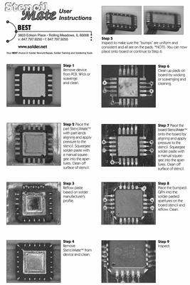
Simplify and Speed Up QFN and LGA device rework. StencilMate™ leadless device rework stencils make the process of reworking leadless devices such as QFNs and LGAs simple and fast. These adhesive-backed poyimide stencils are placed on to the bottom o
New Equipment | Assembly Services
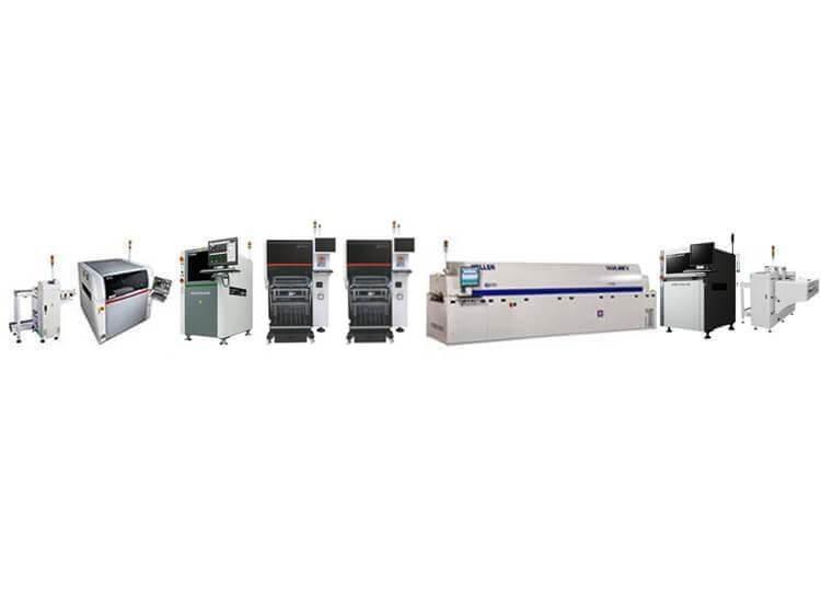
Hanwha HM520 SMT Assembly Line Hanwha HM520 SMT Assembly Line, Usage: PCB production, Full Automatic Assembly line, Speed: 80000CPH, it's with Automatic PCB Loader, Automatic SMT stencil Printer, Koh Young KY 8080 3D SPI, Automatic Pick and place ma
Used SMT Equipment | Soldering - Wave
Working width: 330 mm (13") Solder module: Type: lead-free double wave solder module Solder volume: approx. 390 kg (860 lb.) LEADFREE approx. 335 kg (739 lb.) lead-free alloy Warm-up time: approx. 2.5 h Preheating length: 1,100 mm (43.3") Fl

Used SMT Equipment | Soldering - Wave
ERSA Powerflow N2 XL Wave Solder Machine (2011) Brand: Ersa Model : Powerflow N2 XL Serial #: W039A-11K0015 Year: 2011 Type : Wave Solder Machine Voltage: 400V Power Supply: 3 Phase Exhaust: 800/ 2 x 200m³ Weight: Approx. 3,200 kg CE
Industry News | 2007-11-01 20:29:37.0
November 1, 2007 - Lloyd Doyle announces they will showcase the IBIS system, a brand new development for solder bump inspection, in Hall A1 Stand 347 at the upcoming Productronica 2007 exhibition and conference scheduled to take place November 13-16, 2007 at the Munich Trade Fair Center in Munich, Germany.
Industry News | 2016-02-25 14:29:00.0
SHENMAO Features a new Sn-3.0Ag-0.5Cu Lead-Free Solder Paste PF606-P133H for laser soldering applications. Dispensed from syringes, it is developed for automatic laser soldering processes in the packaging and assembly of surface mount devices and microelectronics. Laser energy is applied at the precise location in a non-contact procedure to create high shear strength well-formed solder joints during the lower thermal stress process while reducing intermetallic formation. PF606-P133H solder paste produces minimal flux residue and no-splash or solder balling issues. It is well suited for high yield soldering of sensitive electronic components in manufacturing or repair of electronic devices that can-not tolerate conventional reflow-oven temperature.
Technical Library | 2023-01-17 17:58:36.0
Heterogeneous integration has become an important performance enabler as high-performance computing (HPC) demands continue to rise. The focus to enable heterogeneous integration scaling is to push interconnect density limit with increased bandwidth and improved power efficiency. Many different advanced packaging architectures have been deployed to increase I/O wire / area density for higher data bandwidth requirements, and to enable more effective die disaggregation. Embedded Multi-die Interconnect Bridge (EMIB) technology is an advanced, cost-effective approach to in-package high density interconnect of heterogeneous chips, providing high density I/O, and controlled electrical interconnect paths between multiple dice in a package. In emerging architectures, it is required to scale down the EMIB die bump pitch in order to further increase the die-to-die (D2D) communication bandwidth. Aa a result, bump pitch scaling poses significant challenges in the plated solder bump reflow process, e.g., bump height / coplanarity control, solder wicking control, and bump void control. It's crucial to ensure a high-quality solder bump reflow process to meet the final product reliability requirements. In this paper, a combined formic acid based fluxless and vacuum assisted reflow process is developed for fine pitch plated solder bumping application. A high-volume production (HVM) ready tool has been developed for this process.
Technical Library | 2016-01-12 11:04:35.0
3D packaging has recently become very attractive because it can provide more flexibility in device design and supply chain, reduce the gap between silicon die and organic substrate, help miniaturize devices and meet the demand of high speed, provide more memory, more function and low cost. With the advancement of 3D packaging, the bump height is now down from 80μ to 10μ. When the bump diameter is 20-40μ and height 10μ, the process and reliability are obvious issues. It is well known that underfill can enhance the reliability for regular flip chip, however underfill won’t help assembly process. In order to resolve some difficulties that 3D packaging faces, YINCAE Advanced Materials, LLC has developed solderable anisotropic conductive adhesives for 3D package applications. In this paper we will discuss the assembly process and reliability in detail.

The PCB Footprint Expert is a powerful CAD library development tool powered by our own proprietary CAD LEAP Technology (Libraries Enhanced with Automated Preferences). It is packed with very powerful advanced library management features that cuts foo
Career Center | Tewksbury, Massachusetts USA | Production
Mycronic is a global high-tech company whose innovative solutions have been advancing electronics technology for over 40 years. Today we continue to grow and serve customers in an expanding variety of industries. What we do impacts the future of tech
Career Center | Toronto,, Ontario Canada | Engineering,Research and Development
DEBTANU BASU 40 Fountain Head Road Toronto, ON M3J2V1 (416) 514 0619 Cell: 416 258 7488 E-mail: debtanubasu@aol.com With more than six years of experience in the field of flip chip technologies seeking a challenging technical position in the field
Career Center | Thane, INDIA India | Maintenance,Production,Technical Support
Experience: 12 years relevant work experience in repotted electronic manufacturing industries that includes Data Communications, Consumer Electronics and PC Manufacturing Industry. Work experience in Engineering process and Quality Control. Technica
PCB Libraries, Inc. | https://www.pcblibraries.com/Forum/maximum-height-in-footprint-naming-convention_topic2487_post10249.html
. However, they always provide the maximum height dimension even if they provide the Nominal + tolerance. So basically every component datasheet
Heller Industries Inc. | https://hellerindustries.com/wp-content/uploads/2022/06/Vacuum-Fluxless-Reflow-Technology-for-Fine-Pitch.pdf
) communication bandwidth. Aa a result, bump pitch scaling poses significant challenges in the plated solder bump reflow process, e.g., bump height / coplanarity control, solder wicking control, and bump void control


