Industry Directory | Manufacturer
Reflow ovens for automated SMT PCB assembly, specializing in lead free processing and nitrogen reflow. The best convection reflow ovens on the market.
Industry Directory | Manufacturer / Other
Reduce electrical overstress (EOS) with our EMI filters for soldering, power, ground and servo motors. EMI filters improve equipment up-time and reliability and reduce test problems.
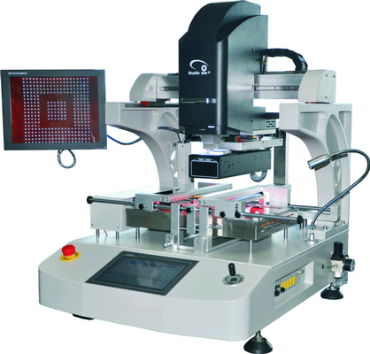
New Equipment | Rework & Repair Equipment
NEW! Nitrogen Capable for High Yield Lead Free BGA Rework. NEW! Movable top and bottom gas heaters allows for easy rework near the edge and hard to ger area's of large PCB's. For high volume BGA Rework on even the largest computer and networking b
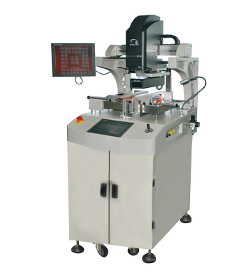
New Equipment | Rework & Repair Equipment
NEW! Nitrogen Capable for High Yield Lead Free BGA Rework NEW! Movable top and bottom gas heaters. NEW! All Shuttle Star BGA Rework Stations are now available with Cabinet Base on wheels. For high volume BGA Rework on even the largest computer a
Electronics Forum | Wed Jul 22 13:50:49 EDT 1998 | Justin Medernach
| My firm has just begun it's first PCB that will use BGA packaging. I have been reading up on the processes involved with BGAs and was wondering if you need to apply solder paste to the pads prior to applying heat and mounting the part to the board
Electronics Forum | Tue Jul 28 16:37:24 EDT 1998 | Terry Burnette
| I think that in general it's best to deposit paste in order to increase the part standoff. This helps improve the fatigue-life of the joints by providing more strain relief. But I know from experience that it's tough to deposit paste during the r
Used SMT Equipment | Screen Printers
Used MPM UP2000HIE Automatic Solder Paste Printer Specification Board range : 50*50-508*406(mm) Board transmitting speed: 1524mm/second Track from the ground level: 876-1041(mm) Printing area: 457-406(mm) Printing speed: 6.35-305(mm/second) P
.jpg)
Used SMT Equipment | Repair/Rework
Physical Dimensions/Weight - Operating Dimensions (W x D x H) -76” x 28” x 24” - Static Dimensions (W x D x H) -52” x 28” x 24” - Weight - 315 lbs (with s
Industry News | 2021-11-08 14:38:39.0
Heller Industries, a leading supplier of reflow soldering ovens for electronic manufacturing and pressure curing ovens for back-end semicondutor manufacturing, today announced they will be exhibiting their new MK7 reflow oven at the San Diego Conference Center January 25-27, 2022.
Industry News | 2003-03-11 08:45:00.0
CAMtastic DXP is the latest version of Altium's complete CAM verification and editing system that bridges the gap between PCB design and manufacturing and facilitates communication between board designers, fabrication engineers, and their clients.
Parts & Supplies | Solder Paste Mixers
12 2-693-981-01 ..... -.... (UNST6-30) BOLT (UNST6-30), STOPPER 4 UNST6-30 13 2-693-982-01 ........ -..- MAKC1008A ABSORBER (MAKC1008A), SHOCK 4 MAKC1008A 14 2-693-982-11 ........ -..- MAKC1008B ABSORBER (MAKC1008B), SHOCK 4 MAK
Technical Library | 2024-10-26 06:26:24.0
Copper pour is an essential design element in printed circuit boards (PCBs) that enhances thermal management, signal integrity, and electrical grounding. It involves filling unused areas on the board with copper, connecting them to power or ground planes. This feature helps manage heat dissipation, minimizes electromagnetic interference (EMI), and provides stable electrical grounding for complex circuits. While copper pour offers significant benefits, improper implementation may lead to manufacturing challenges like warping or soldering difficulties. This article explores the advantages of copper pour, the potential challenges, and how PCB Power integrates this design feature to optimize performance and durability. With advanced manufacturing processes, PCB Power ensures seamless copper pour integration for prototypes and large-scale production, offering turnkey PCB solutions for various industries.
Technical Library | 2018-09-26 20:33:26.0
Bottom terminated components, or BTCs, have been rapidly incorporated into PCB designs because of their low cost, small footprint and overall reliability. The combination of leadless terminations with underside ground/thermal pads have presented a multitude of challenges to PCB assemblers, including tilting, poor solder fillet formation, difficult inspection and – most notably – center pad voiding. Voids in large SMT solder joints can be difficult to predict and control due to the variety of input variables that can influence their formation. Solder paste chemistries, PCB final finishes, and reflow profiles and atmospheres have all been scrutinized, and their effects well documented. Additionally, many of the published center pad voiding studies have focused on optimizing center pad footprint and stencil aperture designs. This study focuses on I/O pad stencil modifications rather than center pad modifications. It shows a no-cost, easily implemented I/O design guideline that can be deployed to consistently and repeatedly reduce void formation on BTC-style packages.

ACI Technologies Inc. (ACI) is a scientific research corporation dedicated to the advancement of electronics manufacturing processes and materials for The Department of Defense and industry. This video provides an overview of our commercial service

The biggest, baddest, most affordable Nitrogen Capable BGA Rework Station demonstrated by Dennis O'Donnell the BGA Expert! Safe, precision rework for SMD, BGA, and LED chips on boards as large as 36" or more!. The versatile E6250U rework station co
Training Courses | | | PCB Rework and Hand Soldering Courses
The PCB rework and hand soldering courses courses cover techniques of rework and repair of PCBs, BGAs and other electronics assemblies, and teach fundamentals of soldering of electronics assemblies.
Training Courses | | | PCB Rework and Hand Soldering Courses
The PCB rework and hand soldering courses courses cover techniques of rework and repair of PCBs, BGAs and other electronics assemblies, and teach fundamentals of soldering of electronics assemblies.
Career Center | Auckland, New Zealand | Engineering
NAVMAN PCBA NPI Engineer Reporting To: PCBA NPI Technical Leader Primary Objective: Transition of PCBs from R&D design to a manufacturable state conforming to all facets of PCBA production Secondary: Develop DFM & best practice guidelines Res
Career Center | Danville, Illinois USA | Production
http://jobs-watchfiresigns.icims.com/watchfiresigns_jobs/jobs/candidate/job.jsp?jobid=1005&mode=view Overview: Watchfire Signs is a dynamic, exciting place to work. Our process engineers utilize their required Bachelors of Engineering and required
Career Center | THRISSUR, India | Maintenance,Production
HANDLING OF MAINTENANCE Camelot,Mascot, Selective Soldering,Wave Soldering,Aquastorm 200,H-500 HI-Z,Kolb,kerry&PBT,GETECH, ATI 105 & Final Touch 101,Heller,Btu&vapour phase,Shuttle,SRT,ESD ,Electrical maintenance . Knowledge in using SLIM KIC 2000&
Career Center | Laguna, Calabarzon Philippines | Engineering,Maintenance,Production,Technical Support
Base on my experience more on line sustaining and preventive maintenance in equipment and testing machine for electronics and semicon company Some slight skills in surface grinding,soldering and LAN connection and installation. Can submit report
Ground Pours - To Pour Or Not To Pour? Ground Pours - To Pour Or Not To Pour? Copper ground pours are created by filling open unused areas with copper generally on the outer layers of the board then connecting the copper fill with stitching vias
ASYMTEK Products | Nordson Electronics Solutions | https://www.nordson.com/en/divisions/dage/about/news/dr-evstatin-krastev-from-nordson-dage-to-present-two-ground-breaking-x-ray-inspection-studies
Dr Evstatin Krastev from Nordson DAGE to Present Two Ground Breaking X-ray Inspection Studies X-Ray Inspection and Test Products Corporate | Global Directory
| https://www.eptac.com/location/eptac-atlanta-metro-training-center?hsLang=en
EPTAC Atlanta Metro Training Center - EPTAC - Train. Work Smarter. Succeed Looking for solder training standards, manuals, kits, and more


winsouce.jpg)