New Equipment | Assembly Services
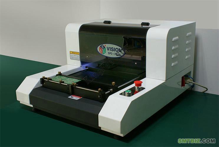
Detailed introduction of 3D spi-7500 solder paste thickness gauge Product function Fast programming, friendly programming interface 1. Multiple measurement methods 2. True one button measurement 3. Eight square movement button, one key foc
New Equipment | Assembly Services
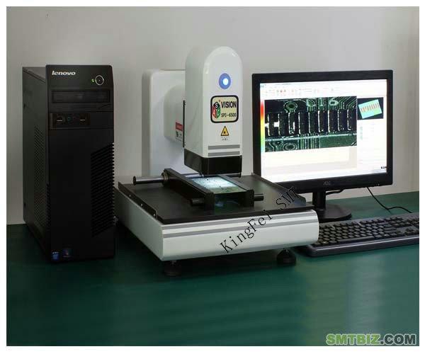
Detailed introduction of 3D spi-6500 solder paste thickness gauge Product function 1. Friendly programming interface 2. Multiple measurement methods 3. The scanning distance is adjustable 4. 3D simulation function of image 5. Independent
Electronics Forum | Wed Dec 12 21:43:16 EST 2007 | davef
There is no specification for solder paste height, just as there is no specification for paste volume. Focus on producing a fillet that meets J-STD-001. You make the choices that produce the end result.
Electronics Forum | Fri May 21 15:50:41 EDT 1999 | John Thorup
We are running a number of boards with 8-10 25 mil PQFPs on board. Our process is mature with at least 3 years experiance and statistically few opens on the QFPs. Our beloved purchasing department has chased the almighty $ and changed FAB vendors
Used SMT Equipment | Soldering - Selective
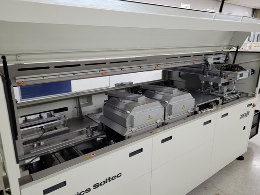
Vitronics Soltec Zeva V Selective Soldering Date of Manufacture: 2018 Details: Inline Preheat Offline Programming Auto Width Adjust SMEMA Interface Advanced Solder Feeder Max PCB: 310 x 410mm Solder Pot Volume: MW 180kg / SW 45kg
Used SMT Equipment | SPI / Solder Paste Inspection
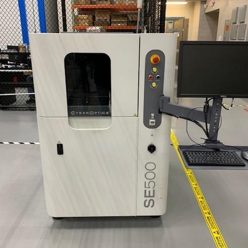
CyberOptics SE500 3D SPI Vintage: 2013 3D Height, Volume, and Area Measurements Max PCB Size: 20" x 20" Min PCB Size: 2" x 2" Complete & Operational
Industry News | 2017-04-03 15:02:09.0
MIRTEC today announced they are participating in the upcoming What's New in Electronics Live! event. They will exhibit in booth #8. They will exhibit in booth #327. The show is scheduled for May 9-10 and will take place at the National Exhibition Center in Birmingham, UK.
Industry News | 2013-03-19 13:24:40.0
Perfect inspection results with combined 2D/3D technology

Parts & Supplies | SPI / Solder Paste Inspection
Quick programming, friendly programming interface Multiple measurement methods True one-button measurement Eight-way motion button, one-click focus Adjustable scanning pitch Solder paste 3D simulation function Powerful SPC function MARK
Parts & Supplies | Soldering Equipment/Fluxes
3D Solder Paste Inspection Machine Features : Easy to use by fully motorize X-Y scan mechanism. Easy to program by Gerber image navigator Easy to repeat the same job by loading the saved program User-friendly color image live view operation Ea
Technical Library | 2023-01-17 17:58:36.0
Heterogeneous integration has become an important performance enabler as high-performance computing (HPC) demands continue to rise. The focus to enable heterogeneous integration scaling is to push interconnect density limit with increased bandwidth and improved power efficiency. Many different advanced packaging architectures have been deployed to increase I/O wire / area density for higher data bandwidth requirements, and to enable more effective die disaggregation. Embedded Multi-die Interconnect Bridge (EMIB) technology is an advanced, cost-effective approach to in-package high density interconnect of heterogeneous chips, providing high density I/O, and controlled electrical interconnect paths between multiple dice in a package. In emerging architectures, it is required to scale down the EMIB die bump pitch in order to further increase the die-to-die (D2D) communication bandwidth. Aa a result, bump pitch scaling poses significant challenges in the plated solder bump reflow process, e.g., bump height / coplanarity control, solder wicking control, and bump void control. It's crucial to ensure a high-quality solder bump reflow process to meet the final product reliability requirements. In this paper, a combined formic acid based fluxless and vacuum assisted reflow process is developed for fine pitch plated solder bumping application. A high-volume production (HVM) ready tool has been developed for this process.
Technical Library | 2013-07-03 10:31:54.0
It has been demonstrated in numerous pieces of work that stencil printing, one of the most complex PCB assembly processes, is one of the largest contributors to defects (Revelino et el). This complexity extends to prototype builds where a small number of boards need to be assembled quickly and reliably. Stencil printing is becoming increasingly challenging as packages shrink in size, increase in lead count and require closer lead spacing (finer pitch). Prototype SMT assembly can be further divided between industrial and commercial work and the DIYer, hobbyist or researcher groups. This second group is highly price sensitive when it comes to the materials used for the board assembly as their funds are sourced from personal or research monies as opposed to company funds. This has led to development of a lower cost SMT printing stencil made from plastic film as opposed to the more traditional stainless steel stencil used by industrial and commercial users.This study compares the performance of these two traditional materials and their respective impact on solder paste printing including efficiency and print quality.
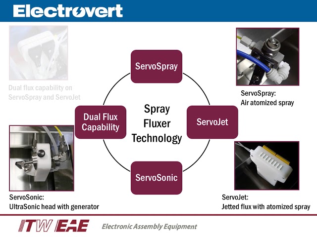
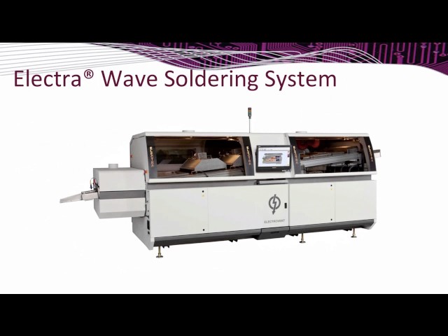
DescriptionThe Electrovert® Electra™ is an advanced, meticulously engineered wave soldering system designed for high-mass and high-volume manufacturers. Although intended for maximum throughput requirements, the Electra also offers maximum process fl
Career Center | Senai, Johor Malaysia | Engineering,Production,Quality Control
A Six Sigma Green Belt practitioner with high experience in process,quality and production engineering.
Career Center | , | Engineering,Production
Project Management, SMT Process Engineering
SMT Express, Volume 2, Issue No. 6 - from SMTnet.com Volume 2, Issue No. 6 Wednesday, June 14, 2000 Featured Article Return to Front Page Process Control for Solder Flux Stacy KaliszMark OwenMVTechnology Ltd. ABSTRACT Flux used in ball grid
SMT Express, Volume 2, Issue No. 3 - from SMTnet.com Volume 2, Issue No. 3 Thursday, March 16, 2000 Featured Article Return to Front Page Stencil Design for Mixed Technology Through-hole / SMT Placement and Reflow by William E. Coleman, Photo
GPD Global | https://www.gpd-global.com/lead-free-solder-paste-dispensing.php
Contacts Technical Support About Company Profile News Events Awards Employment » Applications » Lead Free Solder Paste Dispensing & Leaded Solder Paste Dispensing Lead Free Solder Paste Dispensing vs
Lewis & Clark | https://www.lewis-clark.com/product-tag/selective-solder/
: 310mm x 410mm Solder Pot Volume: MW 180kg / SW 45kg Max Soldering Area: 250mm x 350mm Power: 3 x 400v ~ 50/60Hz N2 Consumption: 75L/Min Max Component Height (Top Side): 120mm Condition: Complete & Operational ~ Very Low Usage (see pics) Location & Shipping


