Industry Directory | Manufacturer
The exclusive supplier of SIPAD Solid Solder Deposit in North America and the only SIPAD Solid Solder Deposit (SSD) coating service bureau in the world.
Industry Directory | Distributor / Manufacturer / Manufacturer's Representative / Standards Setting / Certification / Training Provider
PB Technik supplies SMT equipment and materials to the Polish market. JUKI ERSA EKRA BRADY MARANTZ

The PCB Footprint Expert is a powerful CAD library development tool powered by our own proprietary CAD LEAP Technology (Libraries Enhanced with Automated Preferences). It is packed with very powerful advanced library management features that cuts foo
New Equipment | Education/Training
In this One-Day class you will learn successful techniques to re-ball BGA Components. Both Lead and Lead Free Solder Balls will be covered. The student will have an opportunity to use and evaluate some of the most popular BGA rework fixtures on the
Electronics Forum | Fri Jan 22 16:03:17 EST 2021 | SMTA-64387124
Does anyone see any issues in mixing SMD and NSMD pads within one BGA footprint. We have high current pads which we want to make SMD and the other signal pads to be NSMD
Electronics Forum | Tue Feb 09 16:53:06 EST 2021 | SMTA-64387083
The size of the pad changes among the two. A solder mask defined pad will always be larger than a copper defined by your mask expansion setting. This will affect paste volume, if your standard paste aperture is designed for copper defined pads you m
Industry News | 2003-02-13 08:11:45.0
eSight Can Reduce Time-to-manufacture and Time-to-market by as Much as 80%
Industry News | 2003-03-11 08:45:00.0
CAMtastic DXP is the latest version of Altium's complete CAM verification and editing system that bridges the gap between PCB design and manufacturing and facilitates communication between board designers, fabrication engineers, and their clients.

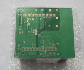
Parts & Supplies | Circuit Board Assembly Products
1). 80 *190mm/2up, FR-4 2). 6 layers at 1.4mm thick 3). 35 μm copper weight 4). Green solder mask LPI/White legend 5). ENIG surface finish 6). Blind via from Layer 1 to layer 2 7). Via in pad plugged conductive resin
Parts & Supplies | Circuit Board Assembly Products
1). 100mm x 98mm/1up, FR-4, 2). 1mm +/-0.1mm,6 Layers 3). 1oz copper finished 3). Green solder mask/white legend 4). Min. hole 0.15mm, 4/4 mil track/gap 5). Blind via layer 1-2, via-in-pad. 6). Immersion gold surface finish
Technical Library | 2007-02-01 10:08:40.0
The increased replacement of high lead count SMT devices with BGAs and other high ball count area array packages has brought increased challenges to PCB rework and repair. Often solder mask areas surrounding BGA pad areas are damaged when components are removed.
Technical Library | 2008-04-08 17:42:27.0
Concern about the failure of lead-free BGA packages when portable devices such as cell phones are accidentally dropped and a general concern about the resistance of these packages under shock loading has prompted an interest in the impact strength of the soldered BGA connection. This paper reports the results of the measurement of the impact strength of lead-free 0.5±0.01mm diameter BGA spheres on 0.42mm solder mask defined pads on copper/OSP and ENIG substrates using recently developed equipment that can load individual BGA spheres at high strain rates in shear and tension.

The PCB Footprint Expert is a powerful CAD library development tool powered by our own proprietary CAD LEAP Technology (Libraries Enhanced with Automated Preferences). It is packed with very powerful advanced library management features that cuts foo
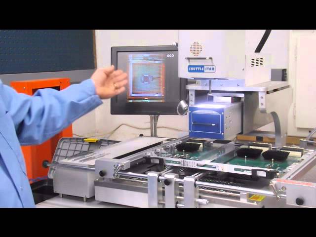
Dennis Odonnell , Vice President of Precision PCB Services, Inc., Oroville CA Explains How to Evaluate a BGA Rework Station ! #BGA Rework Stations http://www.pcb-repair.com/bga-rework-station/
Training Courses | | | PCB Rework and Hand Soldering Courses
The PCB rework and hand soldering courses courses cover techniques of rework and repair of PCBs, BGAs and other electronics assemblies, and teach fundamentals of soldering of electronics assemblies.
Training Courses | | | PCB Rework and Hand Soldering Courses
The PCB rework and hand soldering courses courses cover techniques of rework and repair of PCBs, BGAs and other electronics assemblies, and teach fundamentals of soldering of electronics assemblies.
Events Calendar | Mon Apr 12 00:00:00 EDT 2021 - Mon Apr 12 00:00:00 EDT 2021 | ,
Europe Chapter Webinar: Tombstoning Components during Reflow Soldering - Causes & Cures
Events Calendar | Tue Jan 23 00:00:00 EST 2018 - Tue Jan 23 00:00:00 EST 2018 | New Milford, Connecticut USA
FREE Webinar: Eliminate Circuit Board Problems and Failure Modes
Career Center | Space Coast, Florida USA | Engineering,Research and Development
Board Level Assembly BGA Expert! We are in need of an Electronic Packaging or Advanced Manufacturing Engineer to work with the Advanced Manufacturing Technology Group of a major Florida based Communications company. Support IR&D and Program activit
Career Center | Melbourne, Florida USA | Engineering
Advanced Manufacturing Technology Position Description Job Description: AMT Engineer � Level 4 Support IR&D and Program activities Division wide working on the development, qualification, and implementation of electronic packaging technologies, wi
Career Center | NORTHRIDGE, California USA | Engineering
EDUCATION BS Electronics and Communication Engineering Gujarat University MS Electrical Engineering California State University, Northridge ACADAMIC PROJECT Fabrication and Characterization of Silicon Carbide (SiC) MESFE
ASYMTEK Products | Nordson Electronics Solutions | https://www.nordson.com/en/divisions/efd/resource-center/solder-glossary-of-terms
). Bridging Formation of a solder alloy connection between two or more adjacent contacts. Bumped Circuit Boards Bare printed circuit boards that have had solder paste deposited and reflowed on the pads prior to component installation
Imagineering, Inc. | https://www.pcbnet.com/blog/identifying-and-correcting-solder-bridge-defects/
: No solder mask is present between adjacent pads Spacing of pads is too close Residue accumulation on the surface of a printed circuit board or stencil Misalignment during solder paste printing or


