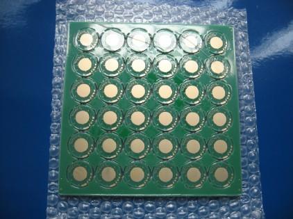
1). 1+C+1 HDI, blind L1-L5/L5-L8 vias. 2). FR-4 Material, 1 oz weight. 3). 8 layer, 1.6mm thick. 4). 4/4 mils track and space 5). Min.drill 0.1mm 6). Green solder mask/ white silkscreen 7). Immersion gold over nickel

New Equipment | Assembly Services
Quick turn Prototype PCBs from 24 hour turnaround to high volume printed circuit board production from our domestic plant in USA and/or China facilities. Our Modern 38,000 sq. ft. manufacturing plant with multi-million dollar investment with latest e
Electronics Forum | Fri Oct 05 07:31:29 EDT 2001 | furrer
When tenting vias almost a few vias are not covered completly by Solder Mask. Does this one side open vias affect the Immersion Tin Process ? Do we get chemical residues in the vias ?
Electronics Forum | Sat Oct 06 08:27:24 EDT 2001 | davef
Yes, some solder masks do not tent well, because the material is too thin. That�s the trade-off. Thin masks: * Conform well to [don't bleed onto] fine pitch features. * Tent vias poorly, requiring an additional "plugging" step. As you imply, if th
Industry News | 2003-03-11 08:45:00.0
CAMtastic DXP is the latest version of Altium's complete CAM verification and editing system that bridges the gap between PCB design and manufacturing and facilitates communication between board designers, fabrication engineers, and their clients.
Industry News | 2018-10-18 10:40:04.0
Via Tent-Holes with Solder Mask
Parts & Supplies | Circuit Board Assembly Products
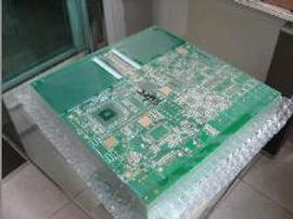
1). 1+C+1 HDI, buried/blind L1-L5/L5-L8 vias. 2). FR-4 Material, 1 oz weight. 3). 8 layer, 1.6mm thick. 4). 4/4 mils track and space 5). Min.drill 0.1mm 6). Green solder mask/ white silkscreen 7). Immersion gold over nickel
Technical Library | 2019-05-29 01:47:22.0
1.Vias near SMD pads: Solder can flow into the via after melted. As a result cold joint will appear in the end. Check the picture below. 2.Vias on SMD pads: Solder can flow into the via more easier after melted. Check the picture below. 3.Via opening without soldermask covered. When workers solder TH parts by hand, soldering iron can touch vias sometime, then tiny amounts molten solder will stay on vias. This can lead to electrical short easily. We recommend you make all vias tenting (covered by solder mask) if it is possible.
PCBNPI-Professional PCB Fab/PCB Assembly Service Provider From China

Events Calendar | Tue Jul 11 00:00:00 EDT 2023 - Tue Jul 11 00:00:00 EDT 2023 | Oshkosh, Wisconsin USA
Wisconsin Chapter In-Person Event: PCB Workshop and PCB Plant Tour
Events Calendar | Wed Sep 11 00:00:00 EDT 2024 - Wed Sep 11 00:00:00 EDT 2024 | Oshkosh, Wisconsin USA
Wisconsin Chapter In-Person Event: PCB Workshop and PCB Plant Tour
PCB Libraries, Inc. | https://www.pcblibraries.com/Forum/qfn-thermal-via-pitch_topic2914.html
. According to the IPC-7093A you can also solder mask define the thermal pad to dam in the paste mask to prevent it from flowing into via holes
Heller Industries Inc. | https://hellerindustries.com/wp-content/uploads/2018/07/00600-248.pdf
M C A N O P T I M I Z E S O L D E R R E F L O W suspended on the bottom purely via surface tension of the solder. Thus, a formula for secondary side mounting can determine a


