
Industry Directory | Equipment Dealer / Broker / Auctions
Our Company handle AOI (Auto Optical Inspection) and SPI (Solder Paste Inspection) Machines.

Industry Directory | Consultant / Service Provider / Manufacturer / Other
ScanCAD is an industry leader in inspection, measurement, process control and reverse engineering. Our solutions support OEM's, manufacturers, stencil fabricators, repair depots, and others in optimizing quality and yield.

New Equipment | Education/Training
IPC - Association Connecting Electronics Industries® offers globally recognized industry-traceable training and certification programs on key Electronics Industry Standards. Blackfox, founded in 1996, is the premier Worldwide Approved IPC Training Ce
New Equipment | Education/Training
Cable Wire Harness Assemblies Training This 4-day, lectured course is a comprehensive, instructor-level certification that teaches inspection and assembly criteria for all three classes of cable and wire harness assembly. This course is based on the
Electronics Forum | Wed Apr 27 11:43:32 EDT 2005 | patrickbruneel
Hi Daan, What we did in the time was pareto analyses on all board designs to determine the critical areas (mainly design errors) and only inspect those specific problem areas. Every batch had a copy of the PC board with problem areas marked and only
Electronics Forum | Mon Apr 25 11:24:31 EDT 2005 | Daan Terstegge
I have a question about inspection, touch-up, and how far you need to go to get a product that meets the required IPC-spec. According to some reports (i.e. "New Study Reveals Component Defect Levels" by Stig Oresjo of Agilent) the average defect leve
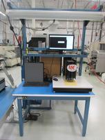
Used SMT Equipment | Visual Inspection
Condition: Complete & Fully Operational
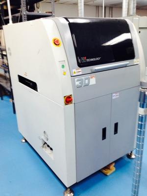
Used SMT Equipment | Visual Inspection
Make: VI Technolgoies Model: 3D XPi 400L Solder Paste Inspection Vintage: 2008 Details: 1. FAHP (flying absolute height profilometry) measurement method 2. Dual light source and on the fly image scan 3. High power M/H light 3D sensor 4. Shadow
Industry News | 2003-03-11 08:45:00.0
CAMtastic DXP is the latest version of Altium's complete CAM verification and editing system that bridges the gap between PCB design and manufacturing and facilitates communication between board designers, fabrication engineers, and their clients.
Industry News | 2013-10-02 14:39:35.0
Baja Bid announced its latest event which features quality used equipment at discounted prices for the electronics manufacturing industry.

Parts & Supplies | Pick and Place/Feeders
KHY-M221A-A0 KGT-M221A-A0 YAMAHA YG12 tank chain gland KHY-M2267-00 YG12 tank chain YS12 towline keel X axis PISCO SP2550 R75 KHY-M2276-S0 YS12 screw X-axis YG12 X-axis screw YG12F YS12F screw guide KHY-M371R-00 RAIL GUIDE 12P YS24 YS100 Feida pl

Parts & Supplies | Visual Inspection
We can supply you the following UNIVERSAL Feeders. Also Feeder Parts, Feeder Storage Carts / Feeder Trolley, Feeder Calibration Jig. 49889209 8mm High Performance DL-60 (Gold Plus) 49889210 8mm High Performance DL-60 (Gold Plus) 49889211 8mm High
Technical Library | 2019-01-02 21:51:49.0
Failed solder joints remain a constant source of printed circuit board failure. Soldering is the bonding of metallic surfaces via an intermetallic compound (IMC). The interaction between thermal energy delivery, flux chemistry, and solder chemistry creates the solder bond or joint. Today, reliability relies on visual inspection; operator experience and skill, control of influencers e.g. tip geometry, tip temperature, and collection and analysis of process data. Each factor involved with the formation of the solder joint is an element of risk and can affect either throughput or repeatability. Mitigating this risk in hand soldering requires the identification of these factors and a means to address them.
Technical Library | 2020-08-27 01:22:45.0
Initially adopted internal specifications for acceptance of printed circuit boards (PCBs) used for wire bonding was that there were no nodules or scratches allowed on the wirebond pads when inspected under 20X magnification. The nodules and scratches were not defined by measurable dimensions and were considered to be unacceptable if there was any sign of a visual blemish on wire-bondable features. Analysis of the yield at a PCB manufacturer monitored monthly for over two years indicated that the target yield could not be achieved, and the main reasons for yield loss were due to nodules and scratches on the wirebonding pads. The PCB manufacturer attempted to eliminate nodules and scratches. First, a light-scrubbing step was added after electroless copper plating to remove any co-deposited fine particles that acted as a seed for nodules at the time of copper plating. Then, the electrolytic copper plating tank was emptied, fully cleaned, and filtered to eliminate the possibility of co-deposited particles in the electroplating process. Both actions greatly reduced the density of the nodules but did not fully eliminate them. Even though there was only one nodule on any wire-bonding pad, the board was still considered a reject. To reduce scratches on wirebonding pads, the PCB manufacturer utilized foam trays after routing the boards so that they did not make direct contact with other boards. This action significantly reduced the scratches on wire-bonding pads, even though some isolated scratches still appeared from time to time, which caused the boards to be rejected. Even with these significant improvements, the target yield remained unachievable. Another approach was then taken to consider if wire bonding could be successfully performed over nodules and scratches and if there was a dimensional threshold where wire bonding could be successful. A gold ball bonding process called either stand-off-stitch bonding (SSB) or ball-stitch-on-ball bonding (BSOB) was used to determine the effects of nodules and scratches on wire bonds. The dimension of nodules, including height, and the size of scratches, including width, were measured before wire bonding. Wire bonding was then performed directly on various sizes of nodules and scratches on the bonding pad, and the evaluation of wire bonds was conducted using wire pull tests before and after reliability testing. Based on the results of the wire-bonding evaluation, the internal specification for nodules and scratches for wirebondable PCBs was modified to allow nodules and scratches with a certain height and a width limitation compared to initially adopted internal specifications of no nodules and no scratches. Such an approach resulted in improved yield at the PCB manufacturer.

ACI Technologies Inc. (ACI) is a scientific research corporation dedicated to the advancement of electronics manufacturing processes and materials for The Department of Defense and industry. This video provides an overview of our commercial service
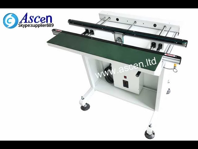
0.5M automatic inspection pcb conveyor and PCB Belt Conveyor|PCB transfer conveyor used for equipment linking, visual inspection, manual assembly, and PCB buffering functions https://www.ascen.ltd/Products/Automatic_SMT_equipment/PCB_conveyor/179.htm
Training Courses | | | IPC J-STD-001 Specialist (CIS)
The Certified IPC J-STD-001 Specialist (CIS) training focuses on the knowledge and hand skills employees need to produce high-quality soldered interconnections.
Training Courses | | | IPC J-STD-001 Space Specialist (CIS)
The J-STD-001 Space Addendum is an additional optional module for the Certified IPC J-STD-001 CIS (Specialist) program for organizations that are required to meet these additional requirements.
Events Calendar | Mon Sep 14 00:00:00 EDT 2020 - Mon Sep 14 00:00:00 EDT 2020 | ,
Printed Circuit Board (PCB) Inspection & Quality Control
Events Calendar | Mon Nov 19 00:00:00 EST 2018 - Mon Nov 19 00:00:00 EST 2018 | ,
Hand Soldering & De-Soldering with Lead-Free Solder - Webinar
Career Center | , Georgia USA | Quality Control
JOB TITLE: QA/SMT Inspection – Electronic PCB Assemblies LOCATIONS: Gwinnett County, GA SHIFT: 2nd Shift 3:30PM – 12:00AM (OT as REQUIRED, possibly including weekends!) STATUS: Indefinite Temporary PAY RATE: $12.00 Hourly Essential Dutie
Career Center | Gwinnett County, Georgia USA | Production
SHIFTS: 1st and 2nd Shifts (Over-Time as required) STATUS: Indefinite Temporary PAY: $11.00-$12.00 per hour JOB DESCRIPTION • Perform SMT soldering, desoldering, rework, and assembly of fine pitch electronic components on Printed Circuit Boards (PCB
Career Center | kishan, India | Engineering,Maintenance,Production,Quality Control,Research and Development
1 year experience as a sales executive,and quality team Leader
Career Center | Poplar Grove, Illinois | Engineering,Production,Quality Control,Technical Support
Please see resume.
SMTnet Express, June 30, 2022, Subscribers: 25,356, Companies: 11,579, Users: 27,312 █ Electronics Manufacturing Technical Articles INTELLI-Pro -- The Future of Automated Optical Inspection In today's Electronics Manufacturing
Lewis & Clark | http://www.lewis-clark.com/product-category/spi/
& Place Press Reflow Oven Rework Station Router Screen Printer Selective Solder Service Spare-Parts SPI- Solder Paste Inspection Systems Uncategorized Wave Solder Wire Bonder X-Ray Contact Us Email Us
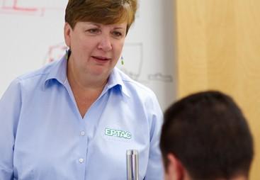
| https://www.eptac.com/ask/visual-acuity-requirements-for-soldering/
Visual Acuity Requirements for Soldering - EPTAC - Train. Work Smarter. Succeed Looking for solder training standards, manuals, kits, and more
Our Company handle AOI (Auto Optical Inspection) and SPI (Solder Paste Inspection) Machines.
Equipment Dealer / Broker / Auctions
Hwaseong-si, Gyeonggi-do, Korea
Hwaseong-si, South Korea
Phone: +82-1029254936


winsouce.jpg)