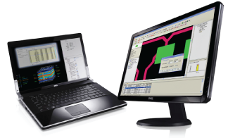
Design For Manufacturability And Yield Enhancement. The Design for Manufacturability (DFM) engine searches for fabrication issues and discovers areas where yields may be increased. GraphiCode's Contour Technology produces fast and accurate results f
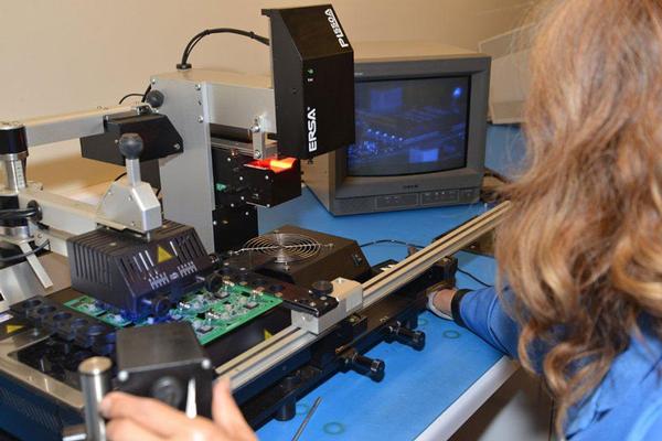
New Equipment | Rework & Repair Services
STI has qualified technicians trained in IPC 7711/7721, as well as in custom design solutions, to address your electronic rework and repair needs. STI’s services encompass both mainstream assembly technologies (surface mount and through-hole) as well
Electronics Forum | Wed Dec 08 19:50:34 EST 2004 | shen_zte
can anyone tell me the benifit of the solder mask onto pad(part) or pad defined by solder mask?and how to excute the SMT process ? thanks.
Electronics Forum | Fri Dec 10 08:42:37 EST 2004 | mattkehoe
We had some bad experiences trying to work with soldermask defined BGA pads. If the opening in the soldermask is right to the edge of the copper/pad without a space it can leave reside on the pad and nothing will stick to it. See http://www.sipad.com
Industry News | 2003-03-11 08:45:00.0
CAMtastic DXP is the latest version of Altium's complete CAM verification and editing system that bridges the gap between PCB design and manufacturing and facilitates communication between board designers, fabrication engineers, and their clients.
Industry News | 2018-10-18 08:32:52.0
How to Prevent Solder Ball and Bridging Defects during the SMT Reflow Process
Technical Library | 2008-04-08 17:42:27.0
Concern about the failure of lead-free BGA packages when portable devices such as cell phones are accidentally dropped and a general concern about the resistance of these packages under shock loading has prompted an interest in the impact strength of the soldered BGA connection. This paper reports the results of the measurement of the impact strength of lead-free 0.5±0.01mm diameter BGA spheres on 0.42mm solder mask defined pads on copper/OSP and ENIG substrates using recently developed equipment that can load individual BGA spheres at high strain rates in shear and tension.
With the development of miniaturization of assembly components, the layout area and pattern design area of PCBs have also been continuously reduced, and PCB manufacturers are constantly updating the production process to conform to the development tr
Training Courses | | | Other Courses
Other courses related to electronics manufacturing and assembly
Training Courses | | | PCB Assembly Courses
The PCB assembly courses provide knowledge of different processes and equipment used in TH and SMT assembly of printed circuit boards.
Events Calendar | Mon Apr 12 00:00:00 EDT 2021 - Mon Apr 12 00:00:00 EDT 2021 | ,
Europe Chapter Webinar: Tombstoning Components during Reflow Soldering - Causes & Cures
Events Calendar | Tue Jan 23 00:00:00 EST 2018 - Tue Jan 23 00:00:00 EST 2018 | New Milford, Connecticut USA
FREE Webinar: Eliminate Circuit Board Problems and Failure Modes
Career Center | Wellsboro, Pennsylvania USA | Engineering
SMT PROCESS ENGINEER: (Wellsboro, PA) - Designs, defines and plans the manufacturing process. Specifies and directs installation of new processes. Plans equipment build schedules and monitors vendor progress. Defines and recommends equipment, methods
SMT Express, Issue No. 2 - from SMTnet.com Volume 1, Issue No. 2 Wednesday, July 14, 1999 Featured Article Continued From Previous Page PRINTED CIRCUIT BOARD FABRICATION BASICS AN OUTLINE Earl Moon Proof Of Design (POD) 8. PLATING (AND
---> SMT Express, Volume 3, Issue No. 6 - from SMTnet.com Volume 3, Issue No. 6 Friday, June 15, 2001 Featured Article Return to Front Page PCB Assembly Techniques by Harvey Twyman , University of Kent at Canterbury "I'm sure you


