New Equipment | Fabrication Services
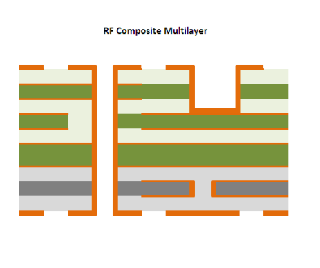
Multilayer PCB's ACI manufactures a wide variety of Multilayer PCB's for various applications spanning numerous industries and technologies. We can build your high layer count PCB's using a wide variety of high speed low loss materials from epoxies
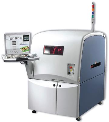
Symbion P36 is an inline high-speed API solution that delivers 100% coverage for improving your product quality and boosting your productivity. Post-Paste AOI Instant Programming Easy Gerber Import 2D/3D Laser Path Superior POP™ D
Electronics Forum | Fri Jan 22 16:03:17 EST 2021 | SMTA-64387124
Does anyone see any issues in mixing SMD and NSMD pads within one BGA footprint. We have high current pads which we want to make SMD and the other signal pads to be NSMD
Electronics Forum | Fri Jan 29 16:17:13 EST 2021 | donnie15
The impact is low on larger pitches and pad sizes. as things get to the .4mm pitch the pad differences start affect your ball size and yields. The trace size going into the pads and the solder mask relief can cause some odd shaped pads with signif
Industry News | 2003-03-11 08:45:00.0
CAMtastic DXP is the latest version of Altium's complete CAM verification and editing system that bridges the gap between PCB design and manufacturing and facilitates communication between board designers, fabrication engineers, and their clients.
Industry News | 2018-10-18 11:08:57.0
What are PCB Thickness Options?
Technical Library | 2019-05-29 01:47:22.0
1.Vias near SMD pads: Solder can flow into the via after melted. As a result cold joint will appear in the end. Check the picture below. 2.Vias on SMD pads: Solder can flow into the via more easier after melted. Check the picture below. 3.Via opening without soldermask covered. When workers solder TH parts by hand, soldering iron can touch vias sometime, then tiny amounts molten solder will stay on vias. This can lead to electrical short easily. We recommend you make all vias tenting (covered by solder mask) if it is possible.
PCBNPI-Professional PCB Fab/PCB Assembly Service Provider From China
Technical Library | 2008-04-08 17:42:27.0
Concern about the failure of lead-free BGA packages when portable devices such as cell phones are accidentally dropped and a general concern about the resistance of these packages under shock loading has prompted an interest in the impact strength of the soldered BGA connection. This paper reports the results of the measurement of the impact strength of lead-free 0.5±0.01mm diameter BGA spheres on 0.42mm solder mask defined pads on copper/OSP and ENIG substrates using recently developed equipment that can load individual BGA spheres at high strain rates in shear and tension.
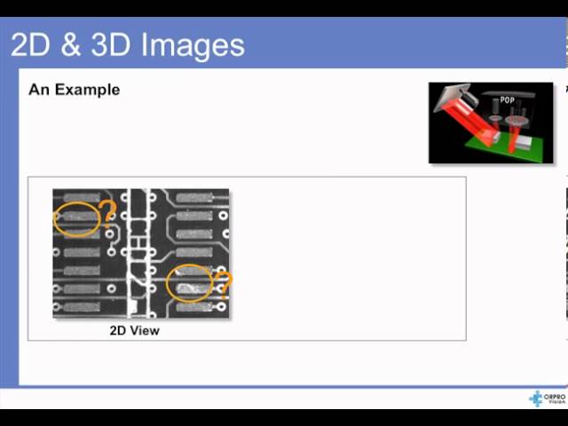
ORPRO Vision SPI Presentation. This presentation introduces the methods and technology used by ORPRO Vision in the Symbion P36 Plus SPI system. For additional information, please contact ORPRO Vision at sales.us@orprovision.com sales.eu@orprovision

SIPAD Systems Incorporated (SSi) is the Exclusive Supplier of SIPAD solid solder deposit in North America and the only SIPAD Solid Solder Deposit (SSD) coating service bureau in the world. SIPAD Systems Inc. supplies SIPAD solid solder coating servi
Events Calendar | Mon Apr 23 00:00:00 EDT 2018 - Thu Apr 26 00:00:00 EDT 2018 | Shanghai, China
SMTA China East Conference 2018
Career Center | Wellsboro, Pennsylvania USA | Engineering
SMT PROCESS ENGINEER: (Wellsboro, PA) - Designs, defines and plans the manufacturing process. Specifies and directs installation of new processes. Plans equipment build schedules and monitors vendor progress. Defines and recommends equipment, methods
SMTnet Express, September 19, 2019, Subscribers: 32,226, Companies: 10,884, Users: 25,126 How Detrimental Production Concerns Related to Solder Mask Residues Can Be Countered by Simple Operational Adaptations Credits: Atotech The symbiotic
PCB Libraries, Inc. | http://www.pcblibraries.com/Products/FPX/PADS-Professional.asp
(Least, Nominal or Most) Silkscreen Line Width and Pad to Silkscreen Gap Minimum Pad to Pad Gap or Pad to Thermal Pad Gap Paste Mask Reduction for Thermal Pads Solder Mask Swell or Solder Mask Defined Pads Map Silkscreen and
| http://etasmt.com/cc?ID=te_news_industry,24564&url=_print
. According to the IPC standard, non-wetting is defined as the inability of molten solder to form a metallic bond with the base metal. This results in the PCB pads or the


