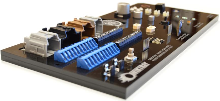
Do you have a unique component that isn’t available in tape and reel? Tired of hand placing those components because you don’t have a compatible feeder? Can’t find JEDEC trays for your components and you need one yesterday? The answer to all of

New Equipment | Rework & Repair Equipment
Ultimate Performance, BGA Rework Station for small-large PCBs up to 24"/620mm The PDR E6 XL BGA Rework Station is made of only the finest materials and components for optimum precision and rework excellence. PDR's E6 SMD Rework Station is PDR's larg
Electronics Forum | Thu Aug 12 17:15:56 EDT 1999 | Jim Blankenhorn
| I am currently involved with designing a pcb which will use 225 pin bga,s | The problem with this design is that the components will dissipate a lot of heat and the design we have come up with is | use the middle 6 or 7 rows of balls as the ground
Electronics Forum | Fri Aug 13 04:12:41 EDT 1999 | ray hare
| | I am currently involved with designing a pcb which will use 225 pin bga,s | | The problem with this design is that the components will dissipate a lot of heat and the design we have come up with is | | use the middle 6 or 7 rows of balls as the
Industry News | 2003-04-15 08:57:18.0
First Implementation of the Package Platform Delivers 50-percent Cost, 60-percent Height, and 75-percent Area Reductions over Conventional RF Module Technologies
Industry News | 2019-05-20 18:57:09.0
SMTA recently released the Guide to BGA Assembly & Soldering Defects, a complimentary resource for the electronics manufacturing industry. The book was written by Keith Bryant, industry veteran and Chairman of the SMTA Europe Chapter, and reviewed by members of the SMTA Europe Technical Committee.
Technical Library | 2023-07-25 16:25:56.0
This paper address two significant applications of stencils in advance packaging field: 1. Ultra-Thin stencils for miniature component (0201m) assembly; 2. Deep Cavity stencils for embedded (open cavity) packaging. As the world of electronics continues to evolve with focus on smaller, lighter, faster, and feature-enhanced high- performing electronic products, so are the requirement for complex stencils to assemble such components. These stencil thicknesses start from less than 25um with apertures as small as 60um (or less). Step stencils are used when varying stencil thicknesses are required to print into cavities or on elevated surfaces or to provide relief for certain features on a board. In the early days of SMT assembly, step stencils were used to reduce the stencil thickness for 25 mil pitch leaded device apertures. Thick metal stencils that have both relief-etch pockets and reservoir step pockets are very useful for paste reservoir printing. Electroform Step-Up Stencils for ceramic BGA's and RF Shields are a good solution to achieve additional solder paste height on the pads of these components as well as providing exceptional paste transfer for smaller components like uBGAs and 0201s. As the components are getting smaller, for example 0201m, or as the available real estate for component placement on a board is getting smaller – finer is the aperture size and the pitch on the stencils. Aggressive distances from step wall to aperture are also required. Ultra-thin stencils with thicknesses in the order of 15um-40um with steps of 15um are used to obtain desired print volumes. Stencils with thickness to this order can be potential tools even to print for RDLs in the package.
Technical Library | 2019-01-30 21:20:47.0
Due to the arrayed nature of the Computed Tomography (CT) Detector, high density area array interconnect solutions are critical to the functionality of the CT detector module. Specifically, the detector module sensor element, hereby known as the Multi-chip module (MCM), has a 544 position BGA area array pattern that requires precise test stimulation. A novel pogo-pin block array and corresponding motorized test socket has been designed to stimulate the MCM and acquire full functional test data. (...) This paper and presentation will focus on the socket design challenges and also key learnings from the design that can be applied to general test systems, including reliability testing. The secondary focus will be on the overall data collection and graphical user interface for the test equipment.
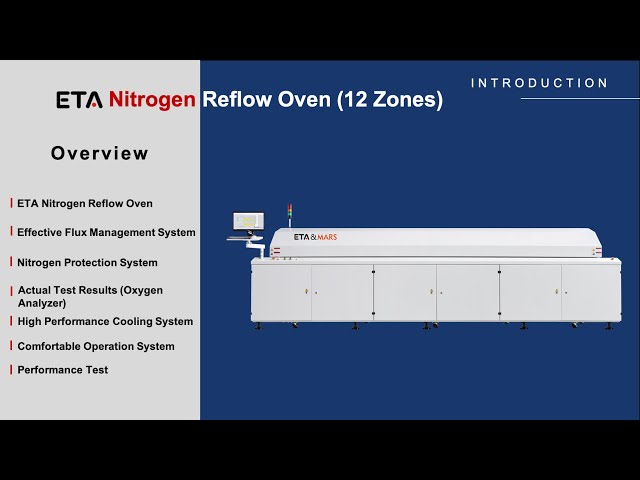
SMT Reflow Ovens for PCB Soldering ❙ Introduce of Reflow Soldering Oven High quality SMT reflow ovens, PCB soldering oven machine, lead-free reflow oven, for PCB soldering. ETA SMT machines manufacturers offers from 6-12 zones good price ref
Good Price Reflow Oven Soldering Machine ❙ Introduce of Reflow Soldering Oven High quality SMT reflow ovens, PCB soldering oven machine, lead-free reflow oven, for PCB soldering. ETA SMT machines manufacturers offers from 6-12 zones good pr
Training Courses | | | PCB Design Courses
The PCB design courses teach students the process, techniques and tools needed to design layout of printed circuit boards.
Career Center | San Jose, California USA | Engineering,Research and Development
www.srqconsultants.com : for job reqs Type of job background: Design for Test (DFT), with ATE Test development experience, and an IC design generalist. Job Summary Must have +5 years industry experience combination in IC Design and ATE test. Som
SMT Express, Issue No. 3 - from SMTnet.com Volume 1, Issue No. 3 Wednesday, August 18, 1999 Featured Article Return to Front Page BGA REWORK Earl Moon Proof Of Design (POD) COMPARE PART SQUARENESS TO BOARD'S SILK-SCREEN OR TRACES A part
| https://www.feedersupplier.com/sale-13119501-fuji-bga-rework-station-pcb-loader-unloader-parts.html
: What can we do for you? A: Total SMT Machines and Solution, professional Technical Support and Service. Q: Are you a trade company or a manufacturer? A
Imagineering, Inc. | https://www.pcbnet.com/blog/pcb-prototyping-what-you-should-be-looking-for/
. You can also check the BGA/QFN (ball grid array/quad flat no-leads) parts box and the AS9100 compliance box. Advertised Specials Watch out for our advertised specials, since these might cover most of your basic specifications and you could get an even better deal from us than you usually do


