
New Equipment | Design Services
Assembly documentation is necessary to capture all of the materials, processes, and final requirements of board-level and system-level assemblies. These drawings convey material sets, approved assembly processes, final inspection requirements, and up
New Equipment | Board Handling - Pallets,Carriers,Fixtures
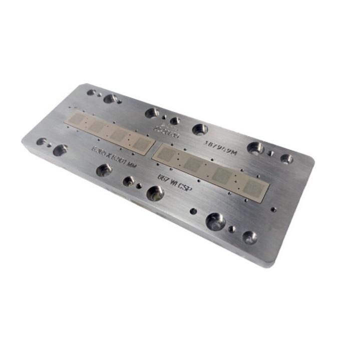
Benefits • Allows testing of RF devices at the wafer-level • Adaptable to wafer-level probing and singulated device testing for debug and characterization • Long life and extended maintenance intervals • Engineering analysis of WLCSP devices or K

Used SMT Equipment | In-Circuit Testers
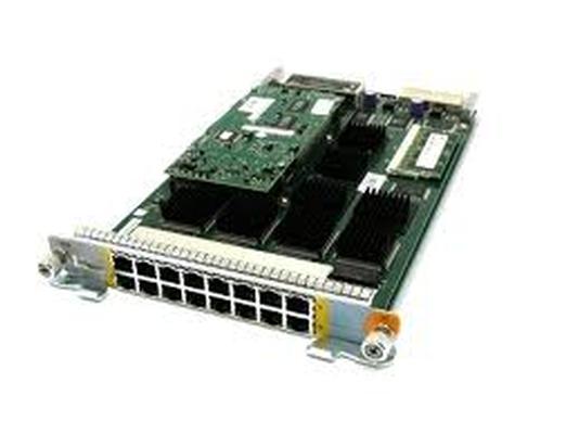
Agilent E7906A 16 Port 10/100 Ethernet Test Card Agilent -Hp E7906A 16 Port 10/100 Ethernet Test Card The RouterTester 10/100 test module has sixteen full-duplex ports. Each port can generate suitably encapsulated IP packets. Many modules can
Used SMT Equipment | In-Circuit Testers
Agilent E7906A 16 Port 10/100 Ethernet Test Card Agilent -Hp E7906A 16 Port 10/100 Ethernet Test Card The RouterTester 10/100 test module has sixteen full-duplex ports. Each port can generate suitably encapsulated IP packets. Many modules can
Industry News | 2019-12-09 14:44:26.0
The SMT Reflow Soldering Equipment (Global) award was awarded to Heller Industries by Frost & Sullivan.
Industry News | 2003-05-28 08:28:54.0
For June 2-4 (Mon. - Wed.)Design Automation Conference 2003
Technical Library | 2009-04-30 18:06:24.0
This presentation surveys the most significant via and via-related laminate failure mechanisms from past to present using data from current induced thermal cycling (CITC) testing, failure analysis, and other sources. The relative life and failure modes of thru vias, buried vias, and microvias (stacked vs. non-stacked) are compared, along with the affect of structure, materials, and peak temperatures on the above. The origin of via-induced laminate failures such as "eyebrow cracks" and Pb free related internal delamination is also explored.
Technical Library | 2016-05-12 16:29:40.0
Advances in miniaturized electronic devices have led to the evolution of microvias in high density interconnect (HDI) circuit boards from single-level to stacked structures that intersect multiple HDI layers. Stacked microvias are usually filled with electroplated copper. Challenges for fabricating reliable microvias include creating strong interface between the base of the microvia and the target pad, and generating no voids in the electrodeposited copper structures. Interface delamination is the most common microvia failure due to inferior quality of electroless copper, while microvia fatigue life can be reduced by over 90% as a result of large voids, according to the authors’ finite element analysis and fatigue life prediction. This paper addresses the influence of voids on reliability of microvias, as well as the interface delamination issue.
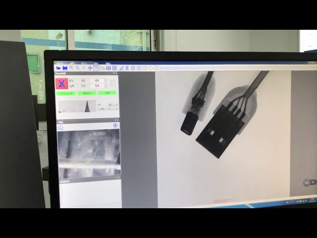
This video presents how to replace and inspect BGA on PCB with our BGA rework station R720 & X ray inspection machine X6600. More details, pls contact me: WhatsApp?+86 18779975930 Skype?joyrongzhuomao@outlook.com Email: sales25@zhuomao.com.cn Link
This video presents how to replace and inspect BGA on PCB with our BGA rework station R720 & X ray inspection machine X6600. More details, pls contact me: WhatsApp?+86 18779975930 Skype?joyrongzhuomao@outlook.com Email: sales25@zhuomao.com.cn Link
Career Center | Fremont, California USA | Engineering
Job Description: • Has full ownership of HW design and release including HW specification creation, schematic generation, PCB layout, board bring up, and design verification. • Complete PCB design schematic using Orcad capture. • Complete HW desig
Career Center | Fremont, California USA | Engineering
Interprets electrical design requirements and uses Allegro design tool to create original PCB layouts, detailed fab drawings, schematics, and other design files. Work with HW design engineer to make sure PCB layout meet PCB design requirements.
Heller Industries Inc. | https://hellerindustries.com/wp-content/uploads/2022/06/Vacuum-Fluxless-Reflow-Technology-for-Fine-Pitch.pdf
. Many factors are considered to control the wicking risk, such as bump metal stack material, bump geometry and Fig. 1 Force analysis at point A; Point A
Baja Bid | https://bajabid.com/an-individual-put-in-gambling-houses-nz-2022-most-beneficial-a-euro-down-payment-online-on-line-casinos-found-at-completely-new-zealand-besides-other-areas/
Asset Management Partner Careers | Current Auctions Linkedin page opens in new window Baja Bid LLC Your EMS Asset Management Partner Home About Services Managed Online Auctions Asset Analysis Consignment Program Cash Buyout Program
.jpg)


