Industry Directory | Consultant / Service Provider
Specialists in high speed serial link architectures by providing innovative signal integrity & backplane solutions
Industry Directory | Consultant / Service Provider
Americom Test provides high speed digital design seminars, private consulting and texts on surface mount technology.

New Equipment | Fabrication Services
Choosing the appropriate material for your printed circuit board is a crucial decision that will impact its suitability for specific applications. Through this blog post, we aim to enhance your understanding of Rogers PCBs. If you require further inf
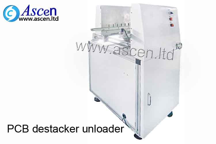
New Equipment | Board Handling - Conveyors
SMT stacking unloader and SMT destacker and PCB destacker is transfering on the electronic assembly line. it can continuously jacking up the PCB board from the belt conveyor one by one and finish unloading operation If you want know more solution
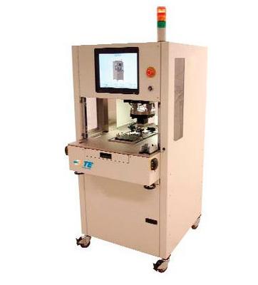
Used SMT Equipment | General Purpose Equipment
Year 2008 - Like New Condition Tyco SEP 3T Shuttle Electric Press Standalone electric press for the application of PCBs onto compliant pin housings or connectors • Servo electric press with shuttle system for product location under press ram • Ho
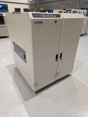
Used SMT Equipment | Conveyors
Nutek Bare Board Loader, XXL size Type: NTM210BXXLBP Serial Nr.: 2013-0578B01 Year of Manufacture: 2013 Direction: Left to Right Fix Rail: Front Transfer height: 900mm (+/-25mm) PCB size: 75 – 600mm (W)/ 150 – 900mm (L) Product thickness: 0.60 – 1.60
Industry News | 2003-04-29 08:27:33.0
Emerson Energy Systems is using Weidmuller's Minimate S2L/B2L PCB connector for its IMT 2000 multifunction unit, thanks to its space saving design and competitive price.
Industry News | 2003-06-10 08:39:25.0
New from Unitek Eapro is a series of desktop systems for hot bar bonding applications.
.png)
Technical Library | 2011-01-20 18:43:39.0
PCB stack-up is an important factor in determining the EMC performance of a product. A good stack-up can be very effective in reducing radiation from the loops on the PCB (differential-mode emission), as well as the cables attached to the board (common-mo
Technical Library | 2008-02-26 15:02:19.0
More and more chip packages need multi-GHz RF structures to meet their performance targets. The ideal chip package needs to combine RF features with Digital features for these applications. They drive low-loss, controlled impedance transmission lines, flexibility in assigned signal and power layers, and clearances of various shapes in power layers. Building these features in a chip package is difficult without making the stack-up very thick or compromising the reliability of the product. In the present paper, we have designed and built a flip-chip package test vehicle (TV) to make new RF structures, using Z-axis interconnection (Zinterconnect) building blocks.
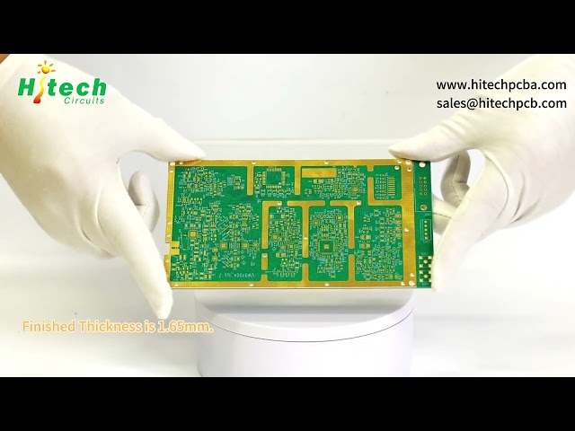
Choosing the appropriate material for your printed circuit board is a crucial decision that will impact its suitability for specific applications. Through this blog post, we aim to enhance your understanding of Rogers PCBs. If you require further inf
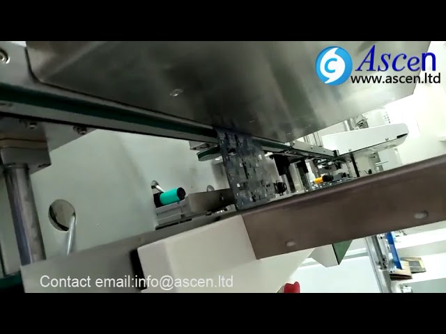
About more detail for the PCB destacker check the link? https://www.ascen.ltd/Products/Automatic_SMT_equipment/PCB_loader/125.html PCB destacker/PCB bare board unloader unloading bare board to replace the PCB magazine unloader machine for the PCB bar
Events Calendar | Mon Jul 10 18:30:00 UTC 2023 - Mon Jul 10 18:30:00 UTC 2023 | Oshkosh, Wisconsin USA
Wisconsin Chapter In-Person Event: PCB Workshop and PCB Plant Tour
Events Calendar | Tue Sep 10 18:30:00 UTC 2024 - Tue Sep 10 18:30:00 UTC 2024 | Oshkosh, Wisconsin USA
Wisconsin Chapter In-Person Event: PCB Workshop and PCB Plant Tour
Career Center | Auckland, New Zealand | Engineering
NAVMAN PCBA NPI Engineer Reporting To: PCBA NPI Technical Leader Primary Objective: Transition of PCBs from R&D design to a manufacturable state conforming to all facets of PCBA production Secondary: Develop DFM & best practice guidelines Res
Career Center | Fremont, California USA | Engineering
Job Description: • Has full ownership of HW design and release including HW specification creation, schematic generation, PCB layout, board bring up, and design verification. • Complete PCB design schematic using Orcad capture. • Complete HW desig
Career Center | Erode, Tamilnadu India | Engineering
Professional Summary 3+ years of experience in the PCB CAM engineering Exposure to FRONTLINE GENESIS 2000 Having exposure in UCAM Exposure to Create, Array & Panelize it for manufacturability Experienced in Creating impedance cou
Career Center | , Israel | Engineering,Maintenance,Technical Support
I was born on June , 1972 in Khmelnitsky city , Ukraine . I am male. From 1979 to 1987 I was studying at secondary school #7, having finished which I entered the Technical College of Khmelnitsky in specialty Machine Tools with Computer Numeric Contr
PCB Libraries, Inc. | https://www.pcblibraries.com/forum/fp-designer-pad-stack-designer_topic3045.html
:15am While preparing one footprint for MPN :821-22-007-10-00010, we found that pad stack designer round-up hole diameter on upper limit. As here
ASCEN Technology | https://www.ascen.ltd/Products/pcb_loader_unloader/306.html
: PCB stacker,PCB destacker,Stack Magazine Loader,stack loader,SMT stacker,SMT destacker,push up stacker,PCB bare board loader save space for loading bare board into the PCB assembly line for the smart factory Send Enquiry Download brochure Product Details Application


