
Industry Directory | Other / Consultant / Service Provider / Manufacturer
ScanCAD is an industry leader in inspection, measurement, process control and reverse engineering. Our solutions support OEM's, manufacturers, stencil fabricators, repair depots, and others in optimizing quality and yield.
Variosystems is among the largest privately owned Contract Electronic Manufacturers worldwide. We offer complete turnkey solutions from engineering to systems integration and order fulfillment.
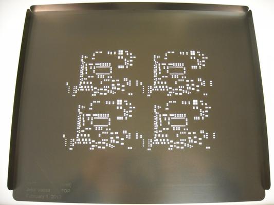
New Equipment | Solder Paste Stencils
Miniature SMT Rework Stencils are laser cut solder paste stencils designed to replicate the intial manufacturing process albeit for a designated component or select area. These laser cut mini stencils can either have flaps (to prevent neighboring are
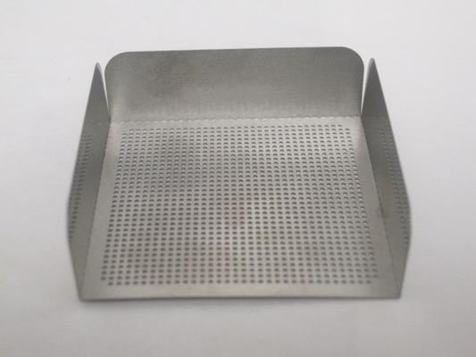
New Equipment | Solder Paste Stencils
SMT Prototype Stencils are laser cut solder paste prototype stencils designed to work on their own for hand printing. These laser cut prototype stencils do not need to be permanently glued in a frame. These so-called framelessstencils are less expens
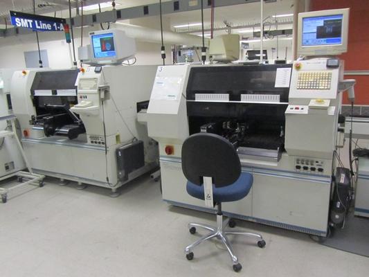
Used SMT Equipment | Screen Printers
DEK Horizon 03i automatic stencil printer Specification : DEK Horizon 03i High Precision Automatic Solder Paste Printer designed for high precision steel mesh printing or stencil printing in SMT industry. Printing PCB size: 50x50mm to 508x510mm;
Used SMT Equipment | Pick and Place/Feeders
Here is your chance to purchase a Fully Automated SMT Line in Good Working Condition at a Low Price Cost new was over $1,000,000+ Million! Equipment consists of the following items DEK 265 GSX Stencil Printer - Green Camera -
Industry News | 2003-03-21 08:12:24.0
Tecan reckons it is consistently producing what may be regarded as the most efficient stencils in the world today.
Industry News | 2016-02-27 20:41:52.0
BEST Inc. instructors will be conducting 2 training sessions this year at the APEX Expo 2016 - Advanced Rework: Hands-on BGA Reballing, Lead-Free Devices, and Fine-Pitch Parts, and the 2nd session - Stencil Printing: Consistent Print Volumes for SMT Rework.
Technical Library | 2023-07-25 16:25:56.0
This paper address two significant applications of stencils in advance packaging field: 1. Ultra-Thin stencils for miniature component (0201m) assembly; 2. Deep Cavity stencils for embedded (open cavity) packaging. As the world of electronics continues to evolve with focus on smaller, lighter, faster, and feature-enhanced high- performing electronic products, so are the requirement for complex stencils to assemble such components. These stencil thicknesses start from less than 25um with apertures as small as 60um (or less). Step stencils are used when varying stencil thicknesses are required to print into cavities or on elevated surfaces or to provide relief for certain features on a board. In the early days of SMT assembly, step stencils were used to reduce the stencil thickness for 25 mil pitch leaded device apertures. Thick metal stencils that have both relief-etch pockets and reservoir step pockets are very useful for paste reservoir printing. Electroform Step-Up Stencils for ceramic BGA's and RF Shields are a good solution to achieve additional solder paste height on the pads of these components as well as providing exceptional paste transfer for smaller components like uBGAs and 0201s. As the components are getting smaller, for example 0201m, or as the available real estate for component placement on a board is getting smaller – finer is the aperture size and the pitch on the stencils. Aggressive distances from step wall to aperture are also required. Ultra-thin stencils with thicknesses in the order of 15um-40um with steps of 15um are used to obtain desired print volumes. Stencils with thickness to this order can be potential tools even to print for RDLs in the package.
Technical Library | 2017-09-28 16:36:33.0
These nano-coatings also refine the solder paste brick shape giving improved print definition. These two benefits combine to help the solder paste printing process produce an adequate amount of solder paste in the correct position on the circuit board pads. Today, stencil aperture area ratios from 0.66 down to 0.40 are commonly used and make paste printing a challenge. This paper presents data on small area ratio printing for component designs including 01005 Imperial (0402 metric) and smaller 03015 metric and 0201 metric chip components and 0.3 mm and 0.4 mm pitch micro BGAs.

BEST manufactures and designs SMT stencils-both metal and plastic film type. This video demonstrates our metal stencil laser. See more on stencils here: http://www.soldertools.net/categories/Metal-Stencils/
BEST manufactures and designs SMT stencils-both metal and plastic film type. This video demonstrates our metal stencil laser. See more on stencils here: http://www.soldertools.net/categories/Metal-Stencils/
Events Calendar | Mon Dec 07 18:30:00 UTC 2020 - Mon Dec 07 18:30:00 UTC 2020 | Online,
SMTA California Technology Day
Events Calendar | Tue May 30 18:30:00 UTC 2023 - Tue May 30 18:30:00 UTC 2023 | Holtsville, New York USA
Long Island Chapter Meeting: Fine Feature Paste Printing, Stencil Design and Solder Technology
Career Center | Puducheery, Tamil nadu India | Production
________________________________________V. KIRUBAKARAN SMT Production Engineer Mobile: +918925842383 | E-Mail: gvkirubakaran@gmail.com Passport Number: M6034648 | Issued date: 05 February 2015 | Expiry date: 05 February 2015 ___________________
Career Center | , Israel | Engineering,Maintenance,Technical Support
I was born on June , 1972 in Khmelnitsky city , Ukraine . I am male. From 1979 to 1987 I was studying at secondary school #7, having finished which I entered the Technical College of Khmelnitsky in specialty Machine Tools with Computer Numeric Contr
SMTnet Express, September 2, 2021, Subscribers: 26,737, Companies: 11,436, Users: 26,825 Tombstoning Of 0402 And 0201 Components: "A Study Examining The Effects Of Various Process And Design Parameters On Ultra-Small Passive Devices
SMTnet Express, April 16, 2020, Subscribers: 35,920, Companies: 10,989, Users: 25,757 Stencil Printing 008004/0201 Aperture Components Credits: ITW EAE This paper will focus on the application requirements of solder printing small aperture designs
| http://etasmt.com/cc?ID=te_news_bulletin,23570&url=_print
• Skips in the printed solder due to blocked stencil aperture • Misaligned solder print • Improper stencil thickness • Inadequate stencil aperture size
Heller Industries Inc. | https://hellerindustries.com/opensor-insufficient-solder/
stencil aperture Misaligned solder print Improper stencil thickness Inadequate stencil aperture size Excessive pad size Via in pad draining solder from interconnection Reflow-related causes of


winsouce.jpg)