New Equipment | Rework & Repair Equipment
BEST HotDots™ are designed to simply and cleanly attach jumper wires on a board. HotDots™ are built to survive at high temperature as both the adhesive and the polyimide material are designed to withstand wash and reflow temperatures. HotDots™ are a
New Equipment | Education/Training
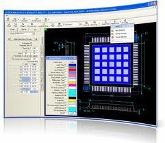
IPC-7351B includes both the standard and an IPC-7351B land pattern calculator on CD-ROM for accessing component and land pattern dimensional data.The calculator includes the document’s mathematical algorithms so users can build a land pattern for a c
Electronics Forum | Tue Jul 19 11:21:50 EDT 2005 | russ
You may want to try reducing the large center aperture on your stencil to 50-70% of the area of the pad. This is what we do with QFNs and it may be applicable in this case also.
Electronics Forum | Wed Oct 11 05:58:13 EDT 2023 | kojotssss
Hello all, I know there are very skilled guys. Can anyone suggest a stencil design to avoid component displacement during reflow to improve tension of surface forces and selfalignment? There are cases where the inductors are shifted. All parameters
Industry News | 2018-10-18 08:40:47.0
Stencil aperture considerations for QFN chips
Industry News | 2009-03-12 18:25:36.0
The SMTA International Technical Committee invites you to submit an abstract for the 2009 conference. Short course descriptions are also being solicited.

Parts & Supplies | Pick and Place/Feeders
Product Description Dear friends, Thanks for your time to visit the page of products introduce. We can provide you nozzle, feeder, filter, guide, belt, cylinder, sensor, bearing, stencil clean roll and other feeder par
Technical Library | 2014-03-13 15:25:01.0
A student competition paper at Budapest University of Technology And Economics, Department of Electronics Technology gives background, covers stencil design and discusses stencils intended for pin in paste application. The stencil applied for depositing the solder paste is a thin, 75–200 µm thick metal foil, on which apertures are formed according to the solder pads on the printed circuit board. Stencil printing provides a fast, mass solder paste deposition process; relatively expensive, appropriate and recommended for mass production.
Technical Library | 2015-08-25 13:51:27.0
The stencil printing process is one of the most critical processes in the electronic production. Due to the requirement: "faster and smaller" it is necessary to place components with different paste volume close together without regard to solder paste printing. In our days it is no longer possible to control the solder paste volume only by adjustment of the aperture dimensions. The requirements of solder paste volumes for specific components are realized by different thicknesses of metal sheets in one stencil with so called step stencils. The step-down stencil is required when it is desirable to print fine-pitch devices using a thinner stencil foil, but print other devices using a thicker stencil foil. The paper presents the innovative technology of step-up and step-down stencils in a laser cutting and laser welding process. The step-up/step-down stencil is a special development for the adjustment of solder paste quantity, fulfilling the needs of placement and soldering. This includes the laser cutting and laser welding process as well as the resulting stencil characteristics and the potential of the printing process.
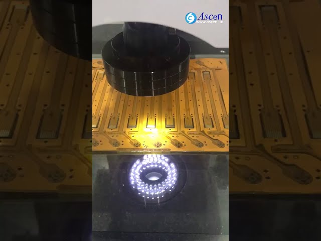
https://www.ascen.ltd/Products/PCB_board_assembly_system/vision_measurin/507.html Vision Measuring Machine and image measuring instrument can be used for dimensional accuracy measurement of various molds, aircraft, automobile, mobile phone, computer,
https://www.ascen.ltd/Products/PCB_board_assembly_system/vision_measurin/507.html Vision Measuring Machine and image measuring instrument can be used for dimensional accuracy measurement of various molds, aircraft, automobile, mobile phone, computer,
Training Courses | | | PCB Rework and Hand Soldering Courses
The PCB rework and hand soldering courses courses cover techniques of rework and repair of PCBs, BGAs and other electronics assemblies, and teach fundamentals of soldering of electronics assemblies.
Events Calendar | Mon Mar 18 00:00:00 EDT 2019 - Mon Mar 18 00:00:00 EDT 2019 | ,
Webinar: Stencil Design for Solder Paste, In Process Inspection & Process Defects
Events Calendar | Mon Apr 23 00:00:00 EDT 2018 - Thu Apr 26 00:00:00 EDT 2018 | Shanghai, China
SMTA China East Conference 2018
Career Center | San Diego, California USA | Engineering,Management,Production
Customer interaction, inventory and delivery of Stencils. In charge of the Satellite Operation in San Diego, Ca. Report to Headquarters in Lake Forest, Ca. Duties and responsibilities: Take full responsibility for the Satellite Operation facility.
Career Center | , Alabama Saudi Arabia | Engineering,Production,Research and Development
SNR MANUFACTURING ENGINEER WANTED Design Change Management and New product Introduction. Solder paste printing process (knowledge of Fuji screen printer machines. Stencil design/ modification and the use of Gerber data. SMT placement machines (Kno
| https://www.feedersupplier.com/sale-13068235-gkg-g5-automatic-smt-screen-printers-smt-stencil-printer.html
. Stencil Cleaner New design of paper over plenum with enhanced vacuum suction gives the best results and ensures no solder paste remains in the stencil apertures
| https://www.smtfactory.com/I-C-T-6534-Solder-Paste-Stencil-Printer-Machine-pd42676824.html
Solder Paste Support Frameless Stencil Printer I.C.T-5151 | Solder Paste PCB SMT Machine Screen Printer Fully Automatic For LED I.C.T-P12 | High Precision Semi-Automatic SMT Screen Stencil Printer in SMD Assembly Line I.C.T-P15 | High Speed SMT Stencil


