Industry Directory | Distributor / Manufacturer
AllPoint Electronics is specialized in SMT, PTH, and TEST Equipment and services for electronics industry in Brazilian market. We provide full support for PCB assembly factory implementation, and process consulting
New Equipment | Solder Paste Stencils
Eliminate hours of solder mask damage repair time for bga sites while improving rework yield. Are you frustrated by the time it takes to repair mask damage underneath the BGA during the rework process? Are you squeezed for space on the PCB in an

New Equipment | Rework & Repair Equipment
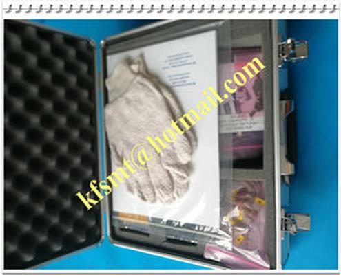
The BEST PCB Epoxy Repair Kit can be used to repair lifted pads and traces as well as build up and repair edge corner damage to PCBs or repair solder mask which has been damaged or removed. By adding colorants a pcb color epoxy kit can be made up cus
Electronics Forum | Tue Feb 03 19:56:43 UTC 2026 | SMTA-81449947
Hello all, I have a PCB I want to run through wave solder with test points(keep out areas) really close to the solder joints. When designing a wave solder pallet, what is the minimum keep out distance from the pallet opening to the desired solder joi

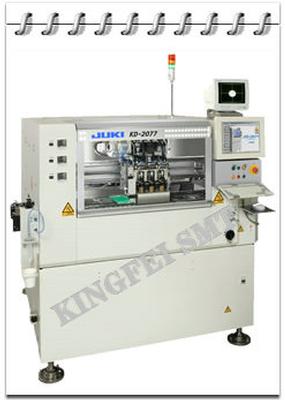
Used SMT Equipment | SMT Equipment
Product name: RX - 6 high-speed module chip mounter Product number: RX - 6 Detailed product introduction Characteristic: With high productivity, versatility, high quality new modular placement machine RX - 6 listed Draw/monitor corresponding p
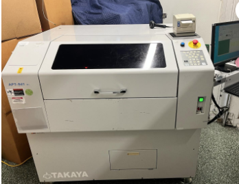
Used SMT Equipment | In-Circuit Testers
Description Make: Takaya Model: APT-9411CE Year: 2010 Type: Flying Probe Details: Takaya APT 9411 CE Flying Probe The APT-9411CE is designed for users who are looking for a precise and reliable test system with an easy to use softwar
Industry News | 2003-06-13 09:56:46.0
Wire and spring specialist William Hughes can now offer three different versions of its PCB test point - small, large and long-legged in quantities suitable for prototype work or volume production.
Industry News | 2003-02-13 08:11:45.0
eSight Can Reduce Time-to-manufacture and Time-to-market by as Much as 80%
Technical Library | 2015-08-20 15:18:38.0
Increasing system integration and component densities continue to significantly reduce the opportunity to access nets using standard test points. Over time the size of test points has been drastically reduced (as small as 0.5 mm in diameter) but current product design parameters have created space and access limitations that remove even the option for these test points. Many high speed signal lines have now been restricted to inner layers only. Where surface traces are still available for access, bead probe technology is an option that reduces test point space requirements as well as their effects on high speed nets and distributes mechanical loading away from BGA footprints enabling test access and reducing the risk of mechanical defects associated with the concentration of ICT spring forces under BGA devices. Building on Celestica's previous work characterizing contact resistance associated with Pr-free compatible surface finishes and process chemistry; this paper will describe experimentation to define a robust process window for the implementation of bead probe and similar bump technology that is compatible with standard Pb-free assembly processes. Test Vehicle assembly process, test methods and "Design of Experiments" will be described. Bead Probe formation and deformation under use will also be presented along with selected results.
Technical Library | 2013-04-04 15:28:39.0
This paper will outline and define what requirements must be adhered to for the OEM community to truly achieve the IPC class product from the Electrical Test standpoint. This will include the test point optimization matrix, Isolation (shorts) parameters and Continuity (opens) parameters. This paper will also address the IPC Class III/A additional requirements for Aerospace and Military Avionics. The disconnect exists between OEMs understanding the requirements of their specific IPC class design versus the signature that will be presented from their design. This results in many Class III builds failing at Electrical Test... First published in the 2012 IPC APEX EXPO technical conference proceedings

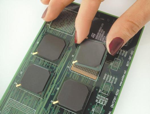
StencilQuik demonstration video. This breakthrough method allows you to simplify placement/replacement saving 50% or more of time required to rework BGAs or CSPs.This is a well developed BGA rework method. More on the StencilQuik(TM) process here:

PCB pad repair technique demonstrated using the 2-part epoxy method. More on this PCB pad repair technique: http://www.solder.net/services/pcb-repair/pad-and-trace-repair/ More on the recommended epoxy: http://www.soldertools.net/pcb-repair-epoxy-r
Training Courses | | | PCB Design Courses
The PCB design courses teach students the process, techniques and tools needed to design layout of printed circuit boards.
Training Courses | | | PCB Design Courses
The PCB design courses teach students the process, techniques and tools needed to design layout of printed circuit boards.
Events Calendar | Mon Jul 10 18:30:00 UTC 2023 - Mon Jul 10 18:30:00 UTC 2023 | Oshkosh, Wisconsin USA
Wisconsin Chapter In-Person Event: PCB Workshop and PCB Plant Tour
Events Calendar | Tue Sep 10 18:30:00 UTC 2024 - Tue Sep 10 18:30:00 UTC 2024 | Oshkosh, Wisconsin USA
Wisconsin Chapter In-Person Event: PCB Workshop and PCB Plant Tour
Career Center | Auckland, New Zealand | Engineering
NAVMAN PCBA NPI Engineer Reporting To: PCBA NPI Technical Leader Primary Objective: Transition of PCBs from R&D design to a manufacturable state conforming to all facets of PCBA production Secondary: Develop DFM & best practice guidelines Res
Career Center | , | 2017-11-02 10:24:18.0
Responsible for construction of prototype circuits/controls, troubleshooting electrical issues and conducting testing to verify electronic design. From schematics, assemble prototype circuits and/or controls to prove out design concepts. Working
Career Center | NORTHRIDGE, California USA | Engineering
EDUCATION BS Electronics and Communication Engineering Gujarat University MS Electrical Engineering California State University, Northridge ACADAMIC PROJECT Fabrication and Characterization of Silicon Carbide (SiC) MESFE
Career Center | , | Engineering,Technical Support
Develop test program, Debug ICT test fixtures, Automated Test Machine and In Circuit Testers. MDA / ICT - Perform Generation of In-Circuit test programs for Tescon (TR-518FR, FE, and 8000i Vacuum type ICT), Teradyne Z1800, Z1803, Conc
SMT Express, Issue No. 2 - from SMTnet.com Volume 1, Issue No. 2 Wednesday, July 14, 1999 Featured Article Continued From Previous Page PRINTED CIRCUIT BOARD FABRICATION BASICS AN OUTLINE Earl Moon Proof Of Design (POD) 8. PLATING (AND
SMTnet Express, December 5, 2019, Subscribers: 32,833, Companies: 10,936, Users: 25,393 Masking for Conformal Coatings Credits: ACI Technologies, Inc. Conformal coatings are regularly employed to protect the surface of a soldered printed circuit
Imagineering, Inc. | https://www.pcbnet.com/blog/understanding-the-pcb-fabrication-process-from-design-to-delivery/
. This information includes the following: Company ID numbers Component references Manufacturer marks or logos Part Numbers Pin locators Switch settings Test points Warning labels Electrical Testing A technician conducts many electrical tests on the PCB
| https://unisoft-cim.com/pcbtest.php
. With over 100 features ProntoVIEW-MARKUP aids every department every day on the shop floor of PCB assembly ( PCBA ) manufacturers where it is used by management, assembly, inspection, design, Test, troubleshooting technicians and other personnel