Industry Directory | Manufacturer
Manufactures and Provides: thermal interface materials (TIM) including insulated-metal-substrates, gap-filling compressible phase-change pads, thermal gels-greases,(EMI/RFI) mitigation conductive gaskets and other products.
Industry Directory | Manufacturer
The exclusive supplier of SIPAD Solid Solder Deposit in North America and the only SIPAD Solid Solder Deposit (SSD) coating service bureau in the world.

The PCB Footprint Expert is a powerful CAD library development tool powered by our own proprietary CAD LEAP Technology (Libraries Enhanced with Automated Preferences). It is packed with very powerful advanced library management features that cuts foo
New Equipment | Fabrication Services
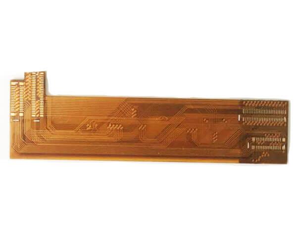
Flexible PCB includes single sided FPC, double sided FPC and multilayer FPC, etc. Single FPC has chemically etched conductive pattern layer, the conductive pattern layer on the surface of the flexible insulating substrate is calendered copper foil. T
Electronics Forum | Tue Feb 01 04:11:58 EST 2000 | emmanuel
I am to assembly a power SO on the top side of a double side board. My designer has implemented a lot of thermal vias in the heat sink pad of this component. The problem is that i need to prevent the solder cream from polluting the bottom side of the
Electronics Forum | Wed Feb 02 03:32:08 EST 2000 | pascal MATHIEU
emmanuel : i agree with Dave , it's easy to have blind hole on the bottom side , of course in this case you'll lose some thermal efficiency ;the second solution is to put on the bottom side between the board and your heatsink a soft thermal interfac
Used SMT Equipment | Soldering - Selective
Pillarhouse Jade MKII Selective Soldering Machine Model: Jade MKII Year: 2016 Lead-Free Drop Jet Fluxer Top Side IR Pre-Heat Auto Soler Top-Up & Solder Level Detect Inerted Nitrogen System Thermal Nozzle Calibrati
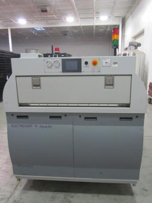
Used SMT Equipment | Board Cleaners
Speedline Technologies AquaJet Stencil Batch Cleaner and Resys ClosedLoop System For Sale The wash needs a control board. (Part Description: BL1700 CNTRL 16IN 16OUT) The Part Number to Purchase this board is 20-101-0214. Estimated cost is $349. We h
Industry News | 2003-03-21 08:12:24.0
Tecan reckons it is consistently producing what may be regarded as the most efficient stencils in the world today.
Industry News | 2003-05-22 08:36:27.0
Packaging Saves PCB Board Space Without Sacrificing Power Dissipation Capability
Parts & Supplies | Pick and Place/Feeders
SMT basic process components include: silk screen (or dispensing), placement (curing), reflow soldering, cleaning, testing, repair 1, silk screen: its role is to paste or patch solder paste printed on the PCB pad, the components f

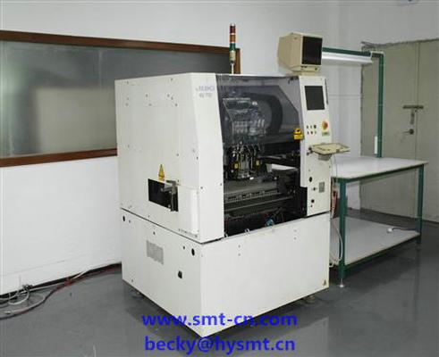
Parts & Supplies | Chipshooters / Chip Mounters
> JUKI ESL13000000 VACUUM PAD 15 JUKI ESL13000100 PHOTO MICRO SENSOR A JUKI ESL13001000 TUBE union (KL700) JUKI ESL130011A0 CONVEYOR MOTOR (KZ500) JUKI ESL13002000 CLAMP LEVER JUKI ESL13003000 T TYPE NUT JUKI ESL130031A0 OPERATION PANEL (KL700) JUKI
Technical Library | 2007-01-31 15:17:04.0
The goal of this project is to evaluate the reliability of lead-free BGA solder joints with a variety of different pad sizes using several different BGA rework methods. These methods included BGAs reworked with both flux only and solder paste attachment techniques and with or without the use of the BEST stay in place StencilQuick™. The daisy chained test boards were placed into a thermal test chamber and cycled between -25ºC to 125ºC over a 30 minute cycle with a 30 minute dwell on each end of the cycle. Each BGA on the board was wired and the continuity assessed during the 1000 cycles the test samples were in the chamber.
Technical Library | 2023-08-04 15:27:30.0
A designed experiment evaluated the influence of several variables on appearance and strength of Pb-free solder joints. Components, with leads finished with nickel-palladium-gold (NiPdAu), were used from Texas Instruments (TI) and two other integrated circuit suppliers. Pb-free solder paste used was tin-silver-copper (SnAgCu) alloy. Variables were printed wiring board (PWB) pad size/stencil aperture (the pad finish was consistent; electrolysis Ni/immersion Au), reflow atmosphere, reflow temperature, Pd thickness in the NiPdAu finish, and thermal aging. Height of solder wetting to component lead sides was measured for both ceramic plate and PWB soldering. A third response was solder joint strength; a "lead pull" test determined the maximum force needed to pull the component lead from the PWB. This paper presents a statistical analysis of the designed experiment. Reflow atmosphere and pad size/stencil aperture have the greatest contribution to the height of lead side wetting. Reflow temperature, palladium thickness, and preconditioning had very little impact on side-wetting height. For lead pull, variance in the data was relatively small and the factors tested had little impact.

The PCB Footprint Expert is a powerful CAD library development tool powered by our own proprietary CAD LEAP Technology (Libraries Enhanced with Automated Preferences). It is packed with very powerful advanced library management features that cuts foo
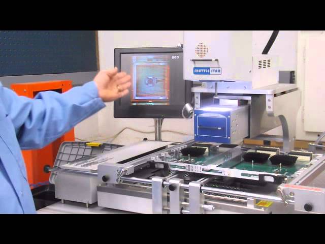
Dennis Odonnell , Vice President of Precision PCB Services, Inc., Oroville CA Explains How to Evaluate a BGA Rework Station ! #BGA Rework Stations http://www.pcb-repair.com/bga-rework-station/
Training Courses | | | PCB Rework and Hand Soldering Courses
The PCB rework and hand soldering courses courses cover techniques of rework and repair of PCBs, BGAs and other electronics assemblies, and teach fundamentals of soldering of electronics assemblies.
Training Courses | | | PCB Rework and Hand Soldering Courses
The PCB rework and hand soldering courses courses cover techniques of rework and repair of PCBs, BGAs and other electronics assemblies, and teach fundamentals of soldering of electronics assemblies.
Career Center | NORTHRIDGE, California USA | Engineering
EDUCATION BS Electronics and Communication Engineering Gujarat University MS Electrical Engineering California State University, Northridge ACADAMIC PROJECT Fabrication and Characterization of Silicon Carbide (SiC) MESFE
Career Center | Phoenix, Arizona | Engineering,Management,Production,Quality Control,Research and Development,Sales/Marketing,Technical Support
• Highly motivated, solution oriented professional with proven record synergizing scientific, engineering, and business administration backgrounds to drive and sustain customer satisfaction and long term improvements. • Articulate communicator that a
Modelling of Thermal Stresses in Printed Circuit Boards Modelling of Thermal Stresses in Printed Circuit Boards Results of FEM modelling of thermal stress analysis in printed circuit boards are given in the article. It is shown that thermal
ORION Industries | http://orionindustries.com/pdfs/thermal.pdf
. Here, Q-Pad II, and Q-Pad 3 grease replacements excel. Both are high performance materials with thermal resistances much lower than Sil-Pad
Imagineering, Inc. | https://www.pcbnet.com/blog/hdi-pcb-advantages-and-applications/
. HDI Features and Benefits Allows designers to incorporate more components onto smaller boards because HDI PCBs can be populated on both sides of the board


winsouce.jpg)