Industry Directory | Manufacturer
As trends towards the miniaturization and increased functional integration of electronics, the demands on quality assurance are rising. FISCHER has many coating thickness measurement solutions for the electronics sector.
Industry Directory | Consultant / Service Provider / Manufacturer
One of the major suppliers of stencils and pallets to the SMT industry. Stentech offers Electroformed and laser cut stencils, pallets and fixtures.

New Equipment | Rework & Repair Equipment
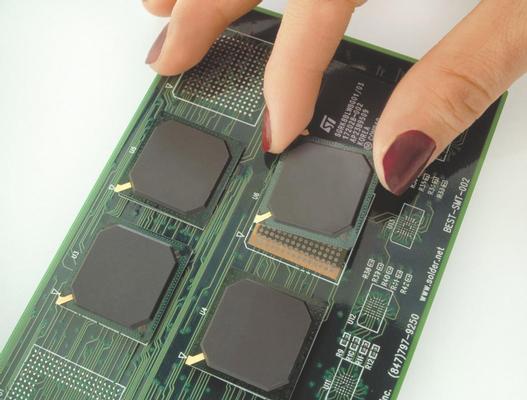
The BEST PCB circuit trace repair kit gives you the tools you need for fast modification and repair of PCB circuit traces. Our online PCB repair training videos, our master instructors along with these materials allows you to meet the original PCB qu
New Equipment | Solder Paste Stencils
Eliminate hours of solder mask damage repair time for bga sites while improving rework yield. Are you frustrated by the time it takes to repair mask damage underneath the BGA during the rework process? Are you squeezed for space on the PCB in an

Used SMT Equipment | AOI / Automated Optical Inspection
SAKI Desktop AOI BF18D-P40 Inspection Machine Substrate flatness: ±2mm Board size:50 * 60 - 250 * 330mm PCB thickness: 0.6mm - 2.5mm weight::30KG ■ Industry-Leading High Throughput Leading High Throughput The Alternate Color Digital Scanning
Used SMT Equipment | Circuit Board Assembly Products
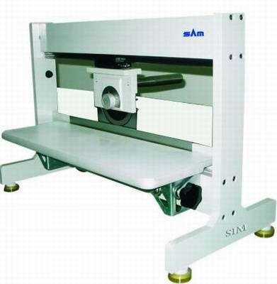
1, Features: SM-2007 separates both small and large pre-scored PCBs. The table and the rest can be continuously adjusted to the most suitable working position, The slit between the linear blade and the rest can be adjusted to ensure that the side s
Industry News | 2003-03-21 08:12:24.0
Tecan reckons it is consistently producing what may be regarded as the most efficient stencils in the world today.
Industry News | 2003-06-18 08:04:27.0
Recently purchased and installed a new DP-1500-2X Dual-Sided Photoimageable Ink Coater from Circuit Automation

Technical Library | 2014-07-02 16:46:09.0
Growth behaviors of intermetallic compounds (IMCs) and Kirkendall voids in Cu/Sn/Cu microbump were systematically investigated by an in-situ scanning electron microscope observation. Cu–Sn IMC total thickness increased linearly with the square root of the annealing time for 600 h at 150°C, which could be separated as first and second IMC growth steps. Our results showed that the growth behavior of the first void matched the growth behavior of second Cu6Sn5, and that the growth behavior of the second void matched that of the second Cu3Sn. It could be confirmed that double-layer Kirkendall voids growth kinetics were closely related to the Cu–Sn IMC growth mechanism in the Cu/Sn/Cu microbump, which could seriously deteriorate the mechanical and electrical reliabilities of the fine-pitch microbump systems
Technical Library | 2012-12-13 21:20:05.0
First published in the 2012 IPC APEX EXPO technical conference proceedings. We investigated the micro-void formation of solder joints after reliability tests such as preconditioning (precon) and thermal cycle (TC) by varying the thickness of Palladium (Pd) in Electroless Nickel / Electroless Palladium / Immersion Gold (ENEPIG) surface finish. We used lead-free solder of Sn-1.2Ag-0.5Cu-Ni (LF35). We found multiple micro-voids of less than 10 µm line up within or above the intermetallic compound (IMC) layer. The number of micro-voids increased with the palladium (Pd) layer thickness. Our results revealed that the micro-void formation should be related to (Pd, Ni)Sn4 phase resulted from thick Pd layer. We propose that micro-voids may form due to either entrapping of volatile gas by (Pd, Ni)Sn4 or creeping of (Pd, Ni)Sn4.

PCB pad circuit repair using epoxy. Using multiple angles including overhead and from both right and left angles the BEST instructor staff demonstrates plainly how to repair a PCB pad using the epoxy method. This method is per IPC 7721 4.4.1. http://

StencilQuik demonstration video. This breakthrough method allows you to simplify placement/replacement saving 50% or more of time required to rework BGAs or CSPs.This is a well developed BGA rework method. More on the StencilQuik(TM) process here:
Imagineering, Inc. | https://www.pcbnet.com/blog/improved-conductive-ink-technology-is-boosting-value-for-all-printed-electronics/
the right application, can help replace bulky and heavier applications. Conductive inks and pastes may also be layered upon a substrate to reduce weight and thickness, but increase the flexibility of the finished product
| https://www.eptac.com/faqs/ask-helena-leo/ask/gullwing-lead-deformation
“…parts or components shall not [D1, D2, D3] be mounted if the part or component lead has nicks or deformation exceeding 10% of the diameter, width, or thickness of the lead except as allow for flattened leads


