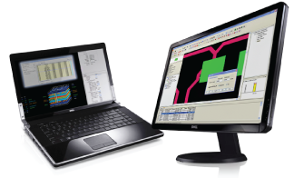
Design For Manufacturability And Yield Enhancement. The Design for Manufacturability (DFM) engine searches for fabrication issues and discovers areas where yields may be increased. GraphiCode's Contour Technology produces fast and accurate results f
Electronics Forum | Sat Apr 19 12:00:07 EDT 2003 | modeltech
I am completely new to SMT design and for my next project I plan to use SMT for the first time. Since production volumes of the PCB's will be low, hand soldering is definitely an option, and will be necessary for my prototype PCB assembly. My proble
Electronics Forum | Wed Jul 03 15:58:16 EDT 2002 | davef
Your thinking is correct. Wave soldering pads that were designed for reflow can create problems: * Large pads used for reflow [too much solder] can create reliability problems. * Bridging [too much solder] creates rework. * Skipping & shadowing from
Industry News | 2009-03-12 18:25:36.0
The SMTA International Technical Committee invites you to submit an abstract for the 2009 conference. Short course descriptions are also being solicited.
Industry News | 2010-02-17 18:45:59.0
The SMTA International Technical Committee invites you to submit an abstract for the 2010 conference. Short course descriptions are also being solicited.
Technical Library | 2023-05-02 19:06:43.0
As 0402 has become a common package for printed circuit board (PCB) assembly, research and development on mounting 0201 components is emerging as an important topic in the field of surface mount technology for PWB miniaturization. In this study, a test vehicle for 0201 packages was designed to investigate board design and assembly issues. Design of Experiment (DOE) was utilized, using the test vehicle, to explore the influence of key parameters in pad design, printing, pick-andplace, and reflow on the assembly process. These key parameters include printing parameters, mounting height or placement pressure, reflow ramping rate, soak time and peak temperature. The pad designs consist of rectangular pad shape, round pad shape and home-based pad shape. For each pad design, several different aperture openings on the stencil were included. The performance parameters from this experiment include solder paste height, solder paste volume and the number of post-reflow defects. By analyzing the DOE results, optimized pad designs and assembly process parameters were determined.
Technical Library | 2024-07-24 01:04:35.0
Quad Flat No Leads (QFN) package designs receive more and more attention in electronic industry recently. This package offers a number of benefits including (1) small size, such as a near die size footprint, thin profile, and light weight; (2) easy PCB trace routing due to the use of perimeter I/O pads; (3) reduced lead inductance; and (4) good thermal and electrical performance due to the adoption of exposed copper die-pad technology. These features make the QFN an ideal choice for many new applications where size, weight, electrical, and thermal properties are important. However, adoption of QFN often runs into voiding issue at SMT assembly. Upon reflow, outgassing of solder paste flux at the large thermal pad has difficulty escaping and inevitably results in voiding. It is well known that the presence of voids will affect the mechanical properties of joints and deteriorate the strength, ductility, creep, and fatigue life. In addition, voids could also produce spot overheating, lessening the reliability of the joints.

Welcome to this Bob Willis Defect of the Month video on BGA inspection, this series of videos were produced for and featured as part of the NPL/IPC video library and examples are taken from the NPL Defect Database. Over the last couple of years there
smeared solder paste pattern. A typical pad size for
| http://etasmt.com/cc?ID=te_news_industry,24361&url=_print
.Print Solder paste on the PCB. Solder paste is a kind mixture of solder alloy and flux. For reflow soldering normally adopt SnAgCu
| https://www.eptac.com/ask/pem-nut-soldering-criteria/
PEM® Nut Soldering Criteria - EPTAC - Train. Work Smarter. Succeed Looking for solder training standards, manuals, kits, and more
.gif)


