Industry Directory | Consultant / Service Provider
A printed circuit board design service bureau located in the great Pacific Northwest. We specialize in large, complex, fast turn designs common in the video processing and data processing industries.
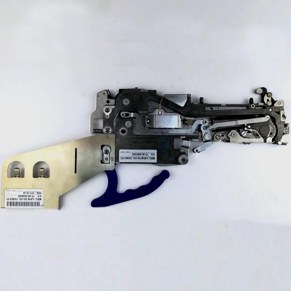
http://www.flason-smt.com/product/YAMAHA-YG12-YG12F-FT8x2mm-Feeder.html YAMAHA YG12 YG12F FT8x2mm Feeder SMT Feeder YAMAHA YG12 YG12F FT8x2mm Feeder KJW-M1100-023 Product description: YAMAHA YG12 YG12F FT8x2mm Feeder KJW-M1100-023 I
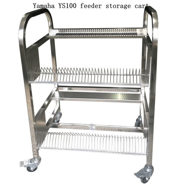
http://www.flason-smt.com/product/Yamaha-YS100-feeder-storage-cart.html Yamaha YS100 feeder storage cart Feeder storage Cart Yamaha Feeder storage Cart Yamaha YS100 feeder storage cart Usage:Yamaha pick and place machine Product description:
Used SMT Equipment | AOI / Automated Optical Inspection
Capture on the fly technology 3D Fusion Lighting (RGB+White LED's) 5 megapixel color imaging 2 top-down and 4 side angle cameras Quick set-up High speed, high defect coverage Low false failure rate Programmable conveyor for boards up to 20 x 2
Used SMT Equipment | Soldering - Reflow
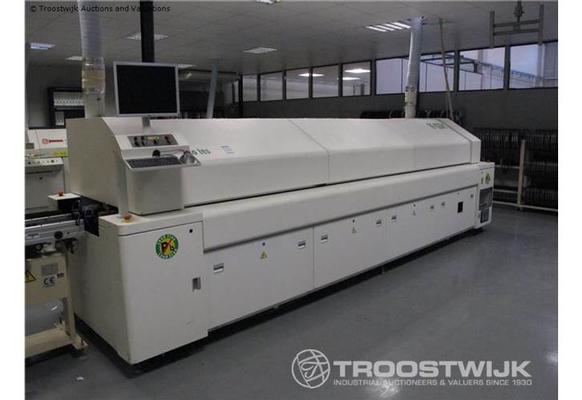
HEXI, Lead-Free reflow soldering machine, type RFN1020/N, s.n. 0611018, Left to Right, with 10 heating heads plus cooling head, lenght of heating zones 3365mm,max width of PCB 450 mm, width of conveyor 50 to 450 mm, height of conveyor 920 +/_ 20 mm,
Industry News | 2010-11-09 19:03:50.0
Count On Tools Inc., a leading provider of precision components and SMT spare parts, will celebrate its 20-year anniversary in 2011.
Industry News | 2012-05-15 11:14:08.0
Tom O’Connor, DFR Solutions, will present a paper on the topic of counterfeit components.
Technical Library | 2020-08-27 01:22:45.0
Initially adopted internal specifications for acceptance of printed circuit boards (PCBs) used for wire bonding was that there were no nodules or scratches allowed on the wirebond pads when inspected under 20X magnification. The nodules and scratches were not defined by measurable dimensions and were considered to be unacceptable if there was any sign of a visual blemish on wire-bondable features. Analysis of the yield at a PCB manufacturer monitored monthly for over two years indicated that the target yield could not be achieved, and the main reasons for yield loss were due to nodules and scratches on the wirebonding pads. The PCB manufacturer attempted to eliminate nodules and scratches. First, a light-scrubbing step was added after electroless copper plating to remove any co-deposited fine particles that acted as a seed for nodules at the time of copper plating. Then, the electrolytic copper plating tank was emptied, fully cleaned, and filtered to eliminate the possibility of co-deposited particles in the electroplating process. Both actions greatly reduced the density of the nodules but did not fully eliminate them. Even though there was only one nodule on any wire-bonding pad, the board was still considered a reject. To reduce scratches on wirebonding pads, the PCB manufacturer utilized foam trays after routing the boards so that they did not make direct contact with other boards. This action significantly reduced the scratches on wire-bonding pads, even though some isolated scratches still appeared from time to time, which caused the boards to be rejected. Even with these significant improvements, the target yield remained unachievable. Another approach was then taken to consider if wire bonding could be successfully performed over nodules and scratches and if there was a dimensional threshold where wire bonding could be successful. A gold ball bonding process called either stand-off-stitch bonding (SSB) or ball-stitch-on-ball bonding (BSOB) was used to determine the effects of nodules and scratches on wire bonds. The dimension of nodules, including height, and the size of scratches, including width, were measured before wire bonding. Wire bonding was then performed directly on various sizes of nodules and scratches on the bonding pad, and the evaluation of wire bonds was conducted using wire pull tests before and after reliability testing. Based on the results of the wire-bonding evaluation, the internal specification for nodules and scratches for wirebondable PCBs was modified to allow nodules and scratches with a certain height and a width limitation compared to initially adopted internal specifications of no nodules and no scratches. Such an approach resulted in improved yield at the PCB manufacturer.
03037000-01 Guide rail 4 left side 03037001-01 Guide rail 5 left side 03037002-01 Guide rail 6 left side 03037017-01 RETRO FIT KIT KGT 20x12 03037268S01 CPU-Bg. SMP16-CPU076 650MHz 128MB 03037619-01 Silencer/Pneumatic System HS
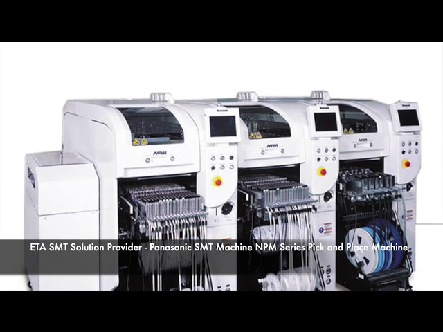
Panasonic AM100 SMT Pick and Place Machine If you could not find any similar items you want, you may send some photos to us. because our catalog and website haven't included allof our products. Pick and place machine, SMT pick and place machine
Events Calendar | Wed Aug 19 18:30:00 UTC 2020 - Wed Aug 19 18:30:00 UTC 2020 | ,
Avoiding the Most Common PCB Failure Modes
| https://www.feedersupplier.com/sale-13119055-yamaha-71f-nozzles-kv8-m71n1-a0x-smt-feeder-parts.html
=0.8 KM4-M7113-10X YV64D DISP. NZ. 2D/2S OD 0.8/ ID 0.5 P=1.0 KM4-M7113-20X YV64D DISP. NZ. 1D/2S OD 0.6/ ID 0.3 KM4-M7113-30X YV64D
1.jpg)
.gif)


