Industry Directory | Manufacturer
Manufacturers flexible printed circuits, circuit materials, IC packaging substrates, laminates, conductive coatings and tapes
Industry Directory | Consultant / Service Provider / Manufacturer
Providing production and prototype, SEC offers advanced technologies like LED thermal management, heavy copper, PTFE for RFMW, open and internal cavities and blind and buried vias that are certified to a diverse set of industries.

The PCB Footprint Expert is a powerful CAD library development tool powered by our own proprietary CAD LEAP Technology (Libraries Enhanced with Automated Preferences). It is packed with very powerful advanced library management features that cuts foo
 -- Hitech Circuits Co., Limited.jpg)
New Equipment | Fabrication Services
We are a professional ceramic pcb manufacturer, supplier from China, we mainly supply high quality Alumina (Al2O3) Ceramic PCB, Aluminum Nitride (AIN) Ceramic PCB board and IGBT Ceramic PCB. Our ceramic printed circuit boards features of high pressur
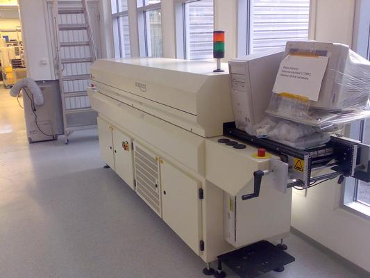
Used SMT Equipment | Soldering - Reflow
The SMRO-4000 Scirocco Reflow oven has been developed for reflow soldering of Hybrid boards, SMT boards and Curing Glue or thin film pastes. The machine is developed for medium to large series of assembly. The Scirocco is based on hot air convection.
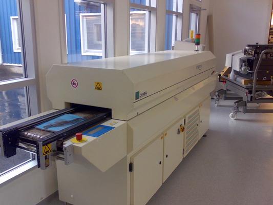
Used SMT Equipment | Soldering - Reflow
The SMRO-4000 Scirocco Reflow oven has been developed for reflow soldering of Hybrid boards, SMT boards and Curing Glue or thin film pastes. The machine is developed for medium to large series of assembly. The Scirocco is based on hot air convection.
Industry News | 2018-04-09 19:48:04.0
SMTA Europe announces Session 1 Technical Program on Predicting Component Life at the “Electronics in Harsh Environments Conference” to be held in Amsterdam, Netherlands, on April 25th, 2018.
Industry News | 2018-10-18 07:56:58.0
Wave soldering process defectives and handling solution

The PCB Footprint Expert is a powerful CAD library development tool powered by our own proprietary CAD LEAP Technology (Libraries Enhanced with Automated Preferences). It is packed with very powerful advanced library management features that cuts foo
PCB Libraries, Inc. | https://www.pcblibraries.com/forum/RSS_copper-on-one-side-of-through-hole_topic1972.xml
. It requires two slotted through holes with no copper on the top side and copper pads on the bottom layer. I have created this pattern several times in FP Designer and it looks good until I try to reload the part either by reloading the FPX or switching to a different part and coming back
Imagineering, Inc. | https://www.pcbnet.com/blog/understanding-the-pcb-fabrication-process-from-design-to-delivery/
. This plating also covers the copper layer, protecting it from oxidation. Many finishing materials currently exist, each with its own set of trade-offs


